background image


Reproduction forbidden without Fibocom Wireless Inc. written authorization - All rights reserved. 

FIBOCOM MC610 Series Hardware Guide 

48/70 


Figure 3-18 Reference circuit of Audio Power Amplifier Output 

3.11 Camera Interface 

MC610 supports two camera interfaces, SPI and MIPI. 

The following table describes the pin description of the CAMERA interface: 

Table 3-22 CAMERA interface 

Pin name 

I/O 

Pin 

Description 

CAM_REFCLK  O 

80 

CAMERA CLK signal 

CAM_PWDN 

79 

CAMERA POWER DOWN signal 

CSI_D0N 

I/O 

92 

CAMERA MIPI data D0 negative terminal; 

CAM_SI1 SPI CAM serial data signal 1 

CSI_D0P 

I/O 

91 

CAMERA MIPI data D0 positive terminal; 

CAM_SCK SPI CAM serial clock signal 

CSI_CKN 

90 

CAMERA MIPI clock CLK negative terminal; 

CAM_RSTL SPI CAM reset signal 

Summary of Contents for MC610 Series

Page 1: ...FIBOCOM MC610 Series Hardware Guide Version V1 0 1 Date 2021 06 23...

Page 2: ...ights reserved FIBOCOM MC610 Series Hardware Guide 2 70 Applicability Type No Product Model Description 1 MC610 LA 00 Support MAIN_ANT FDD GSM Bluetooth 2 MC610 LA 02 Support MAIN_ANT FDD GSM WIFI Sca...

Page 3: ...al is prohibited to excerpt copy any part of or the entire document or transmit the document in any form Notice The document is subject to update from time to time owing to the product version upgrade...

Page 4: ...Hardware Guide 4 70 Change History Version Author Reviewer Approver Update Description V1 0 1 Xu Kaiqiang Wang Liuxia Jin Haibo 2021 06 23 Modify voltage range and RF index add WIFI BT index addition...

Page 5: ...2 Product Specification 11 2 3 Hardware Diagram 12 2 4 Operating Mode 13 3 Application Interface 15 3 1 LCC LGA Interface 15 3 1 1 Pin Distribution 15 3 1 2 Pin Definition 16 3 1 3 Pin Multiplexing 25...

Page 6: ...erface Pin Definition 45 3 10 2 Preventing TDD and Other Noises 46 3 10 3 Handset Interface Circuit 47 3 11 Camera Interface 48 3 12 LCD Interface 49 4 RF Interface 50 4 1 MC610 Working Frequency 50 4...

Page 7: ...served FIBOCOM MC610 Series Hardware Guide 7 70 5 5 ESD Characterization 60 6 Structural Specification 62 6 1 Product Appearance 62 6 2 Structure Size 63 6 3 SMT Paster 63 6 4 Packaging 63 7 Warning 6...

Page 8: ...ture should communicate the following safety instructions to end users If these safety principles are not followed Fibocom Wireless Inc will not be responsible for the consequences caused by incorrect...

Page 9: ...ile terminal equipment when it is near gas stations oil depots chemical plants or explosive workplaces There are potential safety hazards in the operation of electronic devices in any potential explos...

Page 10: ...tic Compatibility EMC requirements for mobile terminals and ancillary equipment l 3GPP TS 27 007 V10 0 8 AT command set for User Equipment UE l 3GPP TS 27 005 V10 0 1 Use of Data Terminal Equipment Da...

Page 11: ...1800 1900 Main Not supported MC610 LA 02 Band 1 2 3 4 5 7 8 28 66 Not supported 850 900 1800 1900 Main WIFI BT Not supported MC610 EU 02 Band1 3 7 8 2 0 28 Not supported 900 1800 Main WIFI BT Not sup...

Page 12: ...and 27 005 and proprietary FIBOCOM AT Firmware update USB Voice service HR FR EFR AMR caller display call transfer call holding call waiting multi party call etc SMS business Point to point MO MT cell...

Page 13: ...th data transmission in the voice call Airplane The RF part of the module does not work only the baseband part works which is equivalent to the function of ordinary MCU Sleep In this mode the module s...

Page 14: ...on forbidden without Fibocom Wireless Inc written authorization All rights reserved FIBOCOM MC610 Series Hardware Guide 14 70 stops working and the serial port is blocked But the VBAT pins are still p...

Page 15: ...ation All rights reserved FIBOCOM MC610 Series Hardware Guide 15 70 3 Application Interface 3 1 LCC LGA Interface MC610 series modules are packaged with LCC 52PIN LGA 76PIN with 128 pins in total 3 1...

Page 16: ...round 8 GND G Ground 9 VBAT PI Vmax 4 2V Vmin 3 4V Vnorm 3 8V VBAT_GSM power input 3 4 to 4 2 V 10 VBAT PI Vmax 4 2V Vmin 3 4V Vnorm 3 8V VBAT_GSM power input 3 4 to 4 2 V 11 USB_DM I O USB signal DM...

Page 17: ...eserve test points 22 GPIO I O 1 8V L GPIO26 Support function U2TXD U3RTS SPI2CLK 23 SIM1_DATA I O 1 8V 3 0V USIM1 data signal line 24 SIM1_CLK O 1 8V 3 0V USIM1 clock signal line 25 SIM1_RST O 1 8V 3...

Page 18: ...VBAT Module reset signal low level valid 38 LPG O 1 8V L Module state representation 39 U2RXD I 1 8V Data receiving of module serial port 2 Multiplexing function KEY_IN1 U2RXD 40 U2TXD O 1 8V Data rec...
Page 19: ...ce clock signal I2C_SCL0 GPIO16 When using GPIO GPIO16 can only be used for output 57 GND G Ground 58 LCD_SIO I O 1 8V 3V Data signal line of LCD SPI Multiplexing function LCD_SIO GPIO0 59 ADC1 I Anal...

Page 20: ...Vnorm 3 8V The battery voltage detection signal should be close to the anode of the battery terminal as far as possible If the charging function is not used it should be connected to VBAT 73 VDRV O Ch...

Page 21: ...e MIC which is not connected internally must receive the HEADMIC signal when using externally 82 I2S2_SDAT_O O 1 8V I2S data output signal Multiplexing function FLSIO1 GPIO3 DSI_D1P I2S2_SDAT_O 83 I2S...

Page 22: ...O 1 8V MIPICSI_CLOCK_P CAM MIPI clock positive terminal Multiplexing function CAM_SI0 CSI_CKP GPIO21 92 CSI_CKN O 1 8V MIPICSI_CLOCK_N CAM MIPI clock negative terminal Multiplexing function CAM_RSTL...

Page 23: ...round 103 SPI_MOSI I 1 8V SPI_MOSI Multiplexing function SPI_MOSI GPIO Keep it floating if not used 104 SPI_CLK O 1 8V SPI_CLK Multiplexing function SPI_CLK GPIO Keep it floating if not used 105 SPI_M...

Page 24: ...1 8V 3V Data transmission of module serial port 2 Multiplexing function GPIO U2TXD 116 GND G Ground 117 GPIO I O 1 8V L GPIO24 Support function SD1_CMD GPIO24 SCL3 118 SDC_CLK SPI2CS_0 O 1 8V SDC_CLK...

Page 25: ...n needs to be changed in the OPEN version l For details of 1 8 V and 3 V high and low level range see Table 5 3 3 1 3 Pin Multiplexing l The above pin definition only represents the default definition...

Page 26: ...ng figure Figure 3 2 Recommended power supply design VBAT power supply needs star route and the filter capacitor design of power supply is shown in the following table Table 3 3 VABT capacitance Recom...

Page 27: ...modules During the design it is necessary to pay special attention to that the ripple wave of power supply is lower than 300 mV line ESR 150 m and ensure that the power supply voltage is not less tha...

Page 28: ...3 4 1 8 V level Parameter Minimum Value Typical Value Maximum Value Unit VDD_IO 1 71 1 8 1 89 V 3 2 3 Power Consumption In the case of 3 8 V power supply the power consumption of MC610 series modules...

Page 29: ...Bm 750 LTE FDD Data transfer Band 8 23dBm 600 LTE FDD Data transfer Band 28 23dBm 600 LTE FDD Data transfer Band 66 23dBm 700 The above results are laboratory test data with a deviation of 10 3 3 Cont...

Page 30: ...for at least 2 s It is recommended to use OC OD drive circuit to control PWRKEY pins The reference circuit is shown in the following figure Figure 3 4 OC OD drive reference startup circuit Another wa...

Page 31: ...RKEY pins VBAT voltage must be stable It is suggested that the interval from VBAT energization to PWRKEY pin lowering should not be less than 30 ms 3 3 1 3 Automatic Startup If the module needs to be...

Page 32: ...of logging off from the base station Hardware shutdown Lowering PWRKEY more than 3 1 s and then releasing Normal shutdown AT shutdown AT CPWROFF Software shutdown 1 When the module works normally do n...

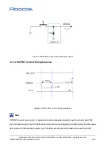
Page 33: ...3 8 Module reset mode Reset Mode Reset Method Hardware reset Provide EXTRST with a Tst 100 ms low level and then rise it AT command reset AT CFUN 15 3 3 3 1 Reset Circuit The reset reference circuit...

Page 34: ...uit 3 3 3 2 EXTRST Control Timing Sequence Figure 3 10 EXTRST control timing sequence EXTRST is a sensitive signal It is suggested to add a debounce capacitor near the module end PCB layout should be...

Page 35: ...pecification 2 0 visit http www usb org home Since the module supports USB 2 0 High Speed the equivalent capacitance of the TVS tube on the USB_DM DP differential signal line is required to be less th...

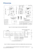
Page 36: ...SIM1_SIO I O 23 USIM SIM1DATA SIM1_CLK O 24 USIM SIM1 Clock Signal SIM1_RST O 25 USIM SIM1 RESET Signal VSIM1 PO 26 USIM SIM1Power SIM1_DET I 27 Detect USIM SIM card for Hot swap SIM2_SIO I O 15 USIM...

Page 37: ...s Inc written authorization All rights reserved FIBOCOM MC610 Series Hardware Guide 37 70 Figure 3 11 Schematic diagram of SIM card slot SIM016 8P 220P Figure 3 12 Reference design diagram for MC610 s...

Page 38: ...a pull up resistor SIM card slot without detection signal module USIM_ PRESENCE pins are subject to 10 kV grounding in series 3 5 3 USIM Design Requirements The circuit design of SIM card needs to co...

Page 39: ...nloading interface UART2 serial port UART3 and serial port DEBUG The main features of four serial ports are described below Main serial ports UART1 and UART3 support the baud rate of 2 400 bps 4 800 b...

Page 40: ...Pin Description U3RXD I 77 Module receiving data U3TXD O 78 Module transmitting data Table 3 14 DEBUG serial port pins Pin Name I O Pin Description DBG_RXD I 94 Module receiving data DBG_TXD O 93 Mod...

Page 41: ...on 1 Another level conversion circuit is shown in the following figure The design of input and output circuits of the following dotted line part can be with reference to the solid line part but pay at...

Page 42: ...ption LPG O 38 Module status indication Description of LPG status of MC610 series module network indicator Table 3 16 LPG status Mode LPG Description 1 Quick flash 600 ms High 600 ms Low No SIM card S...

Page 43: ...ivated by module by the following ways 1 The ATS24 command makes the module to sleep and the wake up keeping time depends on value in the command ATS24 value Send the AT command ATS24 2 The module wil...

Page 44: ...ill be in the sleep mode again after a period of time for wakeup it is 0 by default X 1 level wakeup WAKEUP_IN indicates that sleep is not allowed at low level X 2 level wakeup WAKEUP_IN indicates tha...

Page 45: ...ule has a built in audio encoding and decoding chip provides an analog audio output channel and supports calls and playback and other functions Users can connect SPK directly to the periphery of the m...

Page 46: ...e HEADMIC_N I 100 Earphone MIC input negative HEADMIC_BIAS PO 81 Bias voltage of earphone MIC MIC_P I 29 MIC input positive MIC_N I 28 MIC input negative MIC_BIAS PO 30 MIC bias voltage 8 levels of ga...

Page 47: ...ore serious and in some cases the TDD noise of DCS1800 is more serious Therefore customers can choose the required filter capacitor according to the test results MC615 module has no GSM The RF filter...

Page 48: ...I The following table describes the pin description of the CAMERA interface Table 3 22 CAMERA interface Pin name I O Pin Description CAM_REFCLK O 80 CAMERA CLK signal CAM_PWDN O 79 CAMERA POWER DOWN s...

Page 49: ...he latest MC610 Series Reference Design 3 12 LCD Interface MC610 OPEN can support SPI LCD interface screen The following table shows the pin description of the LCD interface Table 3 23 LCD interface P...

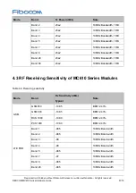
Page 50: ...MHz GSM LTE FDD 1710 1785 1805 1880 Band 4 AWS 1 1700 LTE FDD 1710 1755 2110 2155 Band 5 CLR 850MHz LTE FDD 824 849 869 894 Band 7 IMT E 2600MHz LTE FDD 2500 2570 2620 2690 Band 8 E GSM 900MHz GSM LTE...

Page 51: ...Hz Bandwidth 1 RB Band 28 23 2 10MHz Bandwidth 1 RB Band 66 23 2 10MHz Bandwidth 1 RB 4 3 RF Receiving Sensitivity of MC610 Series Modules Table 4 3 Receiving sensitivity Mode Band Rx Sensitivity dBm...

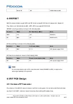
Page 52: ...ity dBm Note WIFI 11b 90 PER 8 BT BLE 91 PER 30 8 BT Transmit Power is shown in the following table Function Mode Tx Power dBm Note BT BLE 6 3 DC power supply 3 8V BT Power Consumption is shown in the...

Page 53: ...hese matches need to be placed close to the antenna Figure 4 1 RF Reference circuit design l Ensure that the characteristic impedance of the transmission line is 50 l As the antenna line loss is less...

Page 54: ...4 Radiation Pattern Radiation pattern refers to the intensity of electromagnetic field in all directions of far field Half wave dipole antenna is the most suitable terminal antenna If it is a built in...

Page 55: ...tion forbidden without Fibocom Wireless Inc written authorization All rights reserved FIBOCOM MC610 Series Hardware Guide 55 70 or filtering processing should be made on the path 7 Antenna Index Requi...

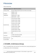
Page 56: ...z GSM1900 PCS 140 MHz Bandwidth LTE LTE band 1 2100 250 MHz LTE Band 2 1900 140 MHz LTE Band 3 1800 170 MHz LTE Band 4 2100 145 MHz LTE Band 5 850 70 MHz LTE Band 7 2500 190 MHz LTE Band 8 900 80 MHz...

Page 57: ...idden without Fibocom Wireless Inc written authorization All rights reserved FIBOCOM MC610 Series Hardware Guide 57 70 Figure 4 2 Design of WiFi reference circuit WiFi only supports WIFI SCAN BT only...

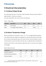
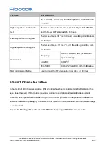
Page 58: ...of digital I O 0 3 2 0 3 2V V 5 2 Ambient Temperature Range MC610 series modules are recommended to work at 30 75 C It is suggested that the temperature control measures should be considered in the a...

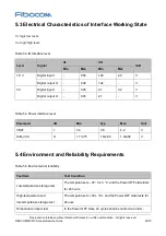
Page 59: ...nput I 0 45 2 1 3 2 V Digital output O 0 45 2 1 V Table 5 4 Power Interface level Parameter I O Min Typ Max Unit VBAT I 3 4 3 8 4 2 V SIM_VCC O 1 7 2 75 1 8 2 85 1 9 2 95 V 5 4 Environment and Reliabi...

Page 60: ...4 hours Vibration test Frequency Random vibration ASD acceleration spectral density 5 to 20Hz 0 96m2 s3 20 to 500Hz 0 96 m2 s3 at 20Hz other 3dB octave Test for connector lifetime Insert and pull the...

Page 61: ...tion All rights reserved FIBOCOM MC610 Series Hardware Guide 61 70 Table 5 6 ESD Characterization Location Air Discharge Contact Discharge GND 15KV 8KV Antenna interface 15KV 8KV Other interfaces 1KV...

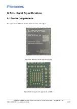
Page 62: ...ization All rights reserved FIBOCOM MC610 Series Hardware Guide 62 70 6 Structural Specification 6 1 Product Appearance The appearance of MC610 series modules is shown in the figure Figure 6 1 Module...

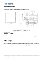
Page 63: ...ing figure Figure 6 3 Structural dimension drawing unit mm 6 3 SMT Paster l Please refer to FIBOCOM MC610 Series SMT Design Guide for module steel mesh design solder paste and furnace temperature cont...

Page 64: ...When testing the host device for compliance with Part 15 Subpart B the host manufacturer is required to show compliance with Part 15 Subpart B while the transmitter module s are installed and operatin...

Page 65: ...the OEM integrator will be responsible for re evaluating the end product including the transmitter and obtaining a separate FCC authorization To comply with FCC regulations limiting both maximum RF ou...

Page 66: ...raged to try to correct the interference by one of the following measures Reorient or relocate the receiving antenna Increase the separation between the equipment and receiver Connect the equipment in...

Page 67: ...ter module may not be co located with any other transmitter or antenna As long as 2 conditions above are met further transmitter test will not be required However the OEM integrator is still responsib...

Page 68: ...S Coding Scheme DRX Discontinuous Reception FDD Frequency Division Duplexing GMSK Gaussian Minimum Shift Keying GSM Global System for Mobile Communications HSDPA High Speed Down Link Packet Access IME...

Page 69: ...U SIM Universal Subscriber Identity Module USSD Unstructured Supplementary Service Data Vmax Maximum Voltage Value Vnorm Normal Voltage Value Vmin Minimum Voltage Value VIHmax Maximum Input High Level...

Page 70: ...rization All rights reserved FIBOCOM MC610 Series Hardware Guide 70 70 Abbreviation Description VSWR Voltage Standing Wave Ratio WCDMA Wideband Code Division Multiple Access 8 2 Contact Company websit...

Reviews: