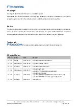


Reproduction forbidden without Fibocom Wireless Inc. written authorization - All Rights Reserved.
FM350-GL Hardware Guide
Page 17 of 59
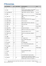
Pin Pin Name
I/O
Reset Value
Pin Description
Level
66 SIM1_DETECT
I
-
SIM1 detect,
internal pull up(390KΩ),
active high
1.8V
67 RESET#
I
PU
WWAN reset input, active low, internal
pull up(35
0KΩ)
1.8V
68 NC
-
-
NC
-
69 CONFIG_1
O
GND
GND, FM350 M.2 module is configured
as the WWAN
– PCIe Gen3, USB3.1
Gen1 interface type
-
70 +3.3V
PI
-
Power input
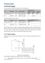
Power Supply
71 GND
-
-
GND
Power Supply
72 +3.3V
PI
-
Power input
Power Supply
73 VIO_CFG
-
NC
Configuration of PCIe sideband signals
power domain
NC: support 1.8V/3.3V;
GND: support 3.3V
-
74 +3.3V
PI
-
Power input
Power Supply
75 CONFIG_2
O
NC
GND, FM350 M.2 module is configured
as the WWAN
– PCIe Gen3, USB3.1
Gen1 interface type
-
Reset Value: The initial status after module reset, not the status when working.
H: High Voltage Level
L: Low Voltage Level
PD: Pull-Down
PU: Pull-Up
T: Tristate
OD: Open Drain
PI: Power Input
PO: Power Output
Note:
Digital IO pins cannot be connected to power directly.
The unused pins can be left floating.


