background image


3 Application Interface 


  Copyright © Fibocom Wireless Inc. 

  42


The  function  of  W_DISABLE1#  is  disabled  in  default.  It  can  be  enabled  by 
customer’s request. 

3.7.2


DPR 

The FM101 module supports BodySAR function by detecting the DPR pin. The voltage level 
of DPR is high by default, and when the SAR sensor detects the closing human body, the 
DPR signal will be pulled down. As the result, the module then lowers down its emission 
power to its default threshold value, thus reducing the RF radiation on the human body. 
The threshold of emission power can be set by the AT Commands. The definition of DPR 
signal is shown in the following table: 

DPR Signal   

Function   

High/Floating 

The module keeps the default emission power 

Low 

Lower the maximum emission power to the threshold value of 
the module. 

3.8


ANT Tunable Interface 

The module supports ANT Tunable interfaces with two different control modes, i.e. MIPI 
interface and 4bit GPO interface. Through cooperating with external antenna adapter 
switch via ANT tunable, it can flexibly configure the bands of WCDMA and LTE antenna to 
improve the antenna’s working efficiency and save space for the antenna. Module also 
support 1.8V output for antenna tuner. The pin definition is as below table: 

Pin    Pin Name   

I/O  Reset Value  Pin Description   

Level 

24 

ANT_TUNER_1V8  PO  PD 

1.8V power output for antenna 
tuner, reserved 

1.8V 

56 

RFFE_SCLK 

O  PD 

Tunable ANT control, MIPI Interface,   

RFFE clock 

1.8V 

Summary of Contents for FM101-GL

Page 1: ...FM101 GL Hardware Guide V1 3...

Page 2: ...g to the product version upgrade or other reasons Unless otherwise specified the document only serves as the user guide All the statements information and suggestions contained in the document do not...

Page 3: ...Features 9 2 4 Application Block 11 2 5 Hardware Block Diagram 12 2 6 Antenna Configuration 13 3 Application Interface 14 3 1 M 2 Interface 14 3 1 1 Pin Map 14 3 1 2 Pin Definition 15 3 2 Power Supply...

Page 4: ...ndicator 40 3 6 1 LED 1 Signal 40 3 7 Interrupt Control 41 3 7 1 W_DISABLE1 41 3 7 2 DPR 42 3 8 ANT Tunable Interface 42 3 9 Configuration Interface 43 4 Radio Frequency 45 4 1 RF Interface 45 4 1 1 R...

Page 5: ...3 M 2 Interface Model 62 6 4 M 2 Connector 63 6 5 M 2 Card Assembly 65 6 5 1 Card Insertion 65 6 5 2 Mid mount Connection with Single Sided Module 65 6 5 1 Top mount Connection with Single Sided Modul...

Page 6: ...Model Copyright Fibocom Wireless Inc 4 Applicable Model No Applicable Model Description 1 FM101 GL 12 Qualcomm SDX12 platform 4G communication module with M 2 interface for Global USB only for data tr...

Page 7: ...differential impedance 90 10 ohms Add USB2 0 and USB3 0 design suggestion Update pin map Update B39 notice B39 support in japan V1 2 2022 01 25 Update USB2 0 description V1 1 2022 01 19 Add notice abo...

Page 8: ...on and reception FDD Part 1 Conformance specification 3GPP TS 34 122 V11 13 0 Technical Specification Group Radio Access Network Radio transmission and reception TDD 3GPP TS 36 521 1 V12 8 0 User Equi...

Page 9: ...AT command set for User Equipment UE 3GPP TS 27 005 V10 0 1 Use of Data Terminal Equipment Data Circuit terminating Equipment DTE DCE interface for Short Message Service SMS and Cell Broadcast Service...

Page 10: ...pecification 2 2 1 RF Characteristic FM101 RF characteristic is shown in Table 1 Table 1 RF characteristic Operating Band FDD LTE B1 2 3 4 5 7 8 12 13 14 17 18 19 20 25 26 28 29 30 66 71 TDD LTE B38 3...

Page 11: ...CC IC 2 Don t support B48 in IC 3 Don t support HPUE in Japan 2 3 Key Features Table 2 Key features Specification CPU Qualcomm SDX12 14nm process ARM Cortex A7 up to 1 28 GHz Memory 2Gb LPDDR2 2Gb NAN...

Page 12: ...2 3 mm Weight TBD Interface Antenna Connector WWAN Antenna x 2 Support 2x2 MIMO Function Interface Dual SIM one embedded eSIM 1 8V 3V USB 2 0 USB 3 0 W_Disable Bodysar LED Tunable antenna I2C Reserve...

Page 13: ...range of 10 C to 55 C RF performance of module may be slightly off 3GPP specifications 2 4 Application Block The peripheral applications for FM101 module are shown in Figure 1 Module SIM1 USB2 0 USB3...

Page 14: ...dware block diagram in Figure 2 shows the main hardware functions of FM101 module including base band and RF functions Baseband contains UMTS LTE TDD LTE FDD controller PMU MCP NAND LPDDR2 Application...

Page 15: ...figuration RX Frequency Range MHz ANT0 M Main antenna port for TRX WCDMA B1 2 4 5 6 8 19 LTE Band B1 2 3 4 5 7 8 12 13 14 17 1 8 19 20 25 26 28 30 66 71 3 8 39 40 41 42 43 48 WCDMA B1 2 4 5 6 8 19 LTE...

Page 16: ...NC NC NC NC I2C_IRQ EINT I2C_SDA I2C Master I2C_SCL I2C Master USB3 0 Tx USB D USB D GND 3 3V NC UIM1_PWR UIM1_DATA UIM1_CLK UIM1_RESET GPIO I W_DISABLE2 3 3 1 8V VIO_1 8V GPIO I W_DISABLE1 3 3 1 8V F...

Page 17: ...is as below table Table 4 IO parameter definition Type Description PI Power Input PO Power Output DI Digital Input DO Digital Output DIO Digital Input Output AI Analog Input AO Analog Output AIO Analo...

Page 18: ...input Power Supply 3 GND GND Power Supply 4 3 3V PI Power input Power Supply 5 GND GND Power Supply 6 FULL_CARD_ POWER_OFF I PU Power enable module power on input internal pull up 3 3 1 8V 7 USB D I...

Page 19: ...01 M 2 module is configured as the WWAN SSIC USB 3 0 interface type 22 GPIO I PD GPIO I default low reserved 1 8V 23 WOWWAN O PD Wake up host default low Reserved 1 8V 24 ANT_TUNER_1V 8 PO PD 1 8V out...

Page 20: ...D GND Power Supply 34 UIM1_DATA I O SIM data input output 1 8V 3V 35 USB 3 0_RX I USB 3 0 receive data minus 36 UIM1_PWR O SIM power supply 1 8V 3V 1 8V 3V 37 USB 3 0_RX I USB 3 0 receive data plus 38...

Page 21: ...ower Supply 52 NC NC 53 NC NC 54 NC NC 55 NC NC 56 RFFE_SCLK O PD MIPI interface tunable ANT RFFE clock 1 8V 57 GND GND Power Supply 58 RFFE_SDATA I O PD MIPI interface tunable ANT RFFE data 1 8V 59 A...

Page 22: ...D Tunable ANT CTRL2 default low 1 8V 64 COEX_TXD O PD Wireless coexistence between WWAN and WIFI BT modules based on BT SIG coexistence protocol UART transmit signal WWAN module side Reserved 1 8V 65...

Page 23: ...type Reset value is the status while module reset not the status in working Digital IO pins cannot be connected to power directly The unused pins can be left floating 3 2 Power Supply The power interf...

Page 24: ...3V The Power rating is shown in the following table Table 7 Power rating 3 2 1 Power Supply The FM101 module should be powered through the 3 3V pins and the power supply design is shown in Figure Pin...

Page 25: ...e stabilizing capacitors Reduce power fluctuations of the module in operation requiring capacitors with low ESR LDO or DC DC power supply requires the capacitor with no less than 440uF in the power su...

Page 26: ...emission power the maximum operating current can reach 2 5A so the power source should be not lower than 3 135V or the module may shut down or reboot The power supply limits are shown in Figure 5 Burs...

Page 27: ...l effective voltage 2 VIH Input high level effective voltage 3 VIL Input low level effective voltage 3 2 3 Power Consumption In the condition of 3 3V power supply the FM101 power consumption is shown...

Page 28: ...Data call Band 6 23 5dBm TBD WCDMA Data call Band 8 23 5dBm TBD WCDMA Data call Band 19 23 5dBm TBD ILTE RMS LTE FDD LTE FDD Data call Band 1 23dBm TBD LTE FDD Data call Band 2 23dBm TBD LTE FDD Data...

Page 29: ...FDD Data call Band 66 23dBm TBD LTE FDD Data call Band 71 24dBm TBD LTE TDD LTE TDD Data call Band 38 23dBm TBD LTE TDD Data call Band 39 23dBm TBD LTE TDD Data call Band 40 23dBm TBD LTE TDD Data cal...

Page 30: ...8V RESET needs to be controlled by independent GPIO and not shared with other devices on the host RESET is sensitive signal so it should be kept away from RF interference and protected by ground It s...

Page 31: ...pulling high FCPO signal After about TBDs module will complete initialization process The start up timing is shown in Figure 3 3V tpr RESET ton Module State Initialization Activation AT Command Ready...

Page 32: ...No response after sent the AT CPWROFF The module can be shut down by sending AT CPWROFF command When the module receives the software shutdown command the module will start the finalization process t...

Page 33: ...20ms and module will restart after RESET signal is released When customer executes RESET function the PMU power will be turned off The recommended circuit design is shown in the Figure 9 Index Min Re...

Page 34: ...1st in Figure 10 PMU of module internal always on in reset sequence recommend using in FW upgrade and module recovery Reset timing 2nd in Figure 11 PMU of module internal will be off in reset sequence...

Page 35: ...fully discharge any residual voltages before the pin could be de asserted again This is required for both Pre OS as well as Runtime flow ton1 8ms 20ms RESET should be de asserted after FCPO assert to...

Page 36: ...cription Type 36 UIM1_PWR PO USIM power supply 1 8V 3V 30 UIM1_RESET O USIM reset 1 8V 3V 32 UIM1_CLK O USIM clock 1 8V 3V 34 UIM1_DATA I O USIM data internal pull up 4 7K 1 8V 3V 66 SIM1_DETECT I PD...

Page 37: ...card is detached it connects the short circuit between CD and SW pins and drives the SIM1_DETECT pin low When the SIM card is inserted it connects an open circuit between CD and SW pins and drives th...

Page 38: ...the description for AT command is shown in the following table AT Command Hot plug Detection Function Description AT MSMPD 1 Enable Default value the SIM card hot plug detection function is enabled T...

Page 39: ...nd UIM_DATA signal lines should be isolated by GND to avoid crosstalk interference If it is difficult for the layout the whole SIM signal lines should be wrapped with GND as a group at least The filte...

Page 40: ...X I USB 3 0 receive data plus 3 5 2 USB2 0 Interface Application The reference circuit is shown in Figure 14 Figure 14 Reference Circuit for USB 2 0 Interface Since the module supports USB 2 0 High Sp...

Page 41: ...3 0_TX USB3 0_TX USB3 0_TX USB3 0_RX USB3 0_RX 0R 0R 100nF 100nF Figure 15 Reference circuit for USB 3 0 interface USB 3 0 signals are super speed differential signal lines with the maximum transfer r...

Page 42: ...lue Pin Description Level 10 LED1 OD T System status LED drain output 3 3V 23 WOWWAN DO PD Wake up host default low Reserved 1 8V 3 6 1 LED 1 Signal The LED 1 signal is used to indicate the operating...

Page 43: ...high active low 3 3 1 8V 25 DPR I PD Dynamic power reduction detect default high active low 3 3 1 8V 3 7 1 W_DISABLE1 The module provides a hardware pin to enable disable WWAN RF function need AT GTF...

Page 44: ...the following table DPR Signal Function High Floating The module keeps the default emission power Low Lower the maximum emission power to the threshold value of the module 3 8 ANT Tunable Interface Th...

Page 45: ...read the level of H L for the host system so the host system can know the module type insert in the M 2 slot If the host system is not need to know the module type that is no need to connect these 4...

Page 46: ...n Type USB 3 0 interface type The M 2 module configuration is shown in the following table Config_0 pin21 Config_1 pin69 Config_2 pin75 Config_3 pin1 Module Type and Main Host Interface Port Configura...

Page 47: ...antenna connection As the Figure 17 shows M is for Main antenna which is used to receive and transmit RF signal D G is for Diversity antenna which is used to receive the diversity RF signal and GNSS s...

Page 48: ...ns FM101 module uses standard M 2 RF connectors The RF connector part number is 818004607 manufactured by ECT cooperation and the size is 2 2 0 6mm The connector dimension is shown as following pictur...

Page 49: ...bly Mate RF connector parallel refer Figure 21 do not slant mate with strong force Figure 21 Mate RF connector To avoid damage in RF connector mating it is recommended using pulling JIG as Figure 22 a...

Page 50: ...3 Lift up pulling JIG Figure 24 Pulling direction 4 2 Operating Band The operating bands of FM101 module are shown in the following table Operating Band Description Mode Tx MHz Rx MHz Band 1 2100MHz L...

Page 51: ...729 746 Band 13 700MHz LTE FDD 777 787 746 756 Band 14 700MHz LTE FDD 788 798 758 768 Band 17 700MHz LTE FDD 704 716 734 746 Band 18 800MHz LTE FDD 815 830 860 875 Band 19 800MHz LTE FDD WCDMA 830 845...

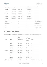
Page 52: ...S L1 1575 42 1 023 GLONASS L1 1602 5625 4 BDS 1561 098 2 046 Galileo 1575 42 1 023 4 3 Transmitting Power The transmitting power for each band of FM101 module is shown in the following table Mode Band...

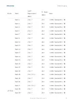
Page 53: ...13 23 2 7 24 1 10MHz Bandwidth 1 RB Band 14 23 2 7 24 1 10MHz Bandwidth 1 RB Band 17 23 2 7 24 1 10MHz Bandwidth 1 RB Band 18 23 2 7 24 1 10MHz Bandwidth 1 RB Band 19 23 2 7 24 1 10MHz Bandwidth 1 RB...

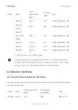
Page 54: ...3 2 3 21 1 10MHz Bandwidth 1 RB 1 B39 TX power is 20 2 7dBm in japan 2 Module default max capability support HPUE The real working mode is decided by NW If NW support HPUE the module can work in HPUE...

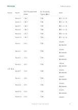
Page 55: ...TBD BER 0 1 Band 6 106 7 TBD BER 0 1 Band 8 103 7 TBD BER 0 1 Band 19 106 7 TBD BER 0 1 LTE FDD Band 1 96 3 TBD 10MHz Bandwidth Band 2 94 3 TBD 10MHz Bandwidth Band 3 93 3 TBD 10MHz Bandwidth Band 4...

Page 56: ...nd 17 93 3 TBD 10MHz Bandwidth Band 18 96 3 TBD 10MHz Bandwidth Band 19 96 3 TBD 10MHz Bandwidth Band 20 93 3 TBD 10MHz Bandwidth Band 25 92 8 TBD 10MHz Bandwidth Band 26 93 8 TBD 10MHz Bandwidth Band...

Page 57: ...andwidth Band 41 94 3 TBD 10MHz Bandwidth Band 42 95 TBD 10MHz Bandwidth Band 43 95 TBD 10MHz Bandwidth Band 48 95 102 10MHz Bandwidth The above values are measured in dual antennas condition Main Div...

Page 58: ...TTFF GPS Cold start TBD Warm start TBD Hot Start TBD GPS BDS GLONASS Galileo Cold start TBD Warm start TBD Hot Start TBD Sensitivity GPS Tracking TBD Acquisition TBD GPS BDS GLONASS Galileo Tracking...

Page 59: ...z WCDMA band 5 850 70 MHz WCDMA band 6 8500 55 MHz WCDMA band 8 900 80 MHz WCDMA band 19 850 60 MHz Bandwidth LTE LTE band 1 2100 250 MHz LTE band 2 1900 140MHz LTE Band 3 1800 170 MHz LTE band 4 1700...

Page 60: ...0 MHz LTE Band 39 1900 40 MHz LTE band 40 2300 100 MHz LTE band 41 2500 194 MHz LTE band 42 3500 200 MHz LTE band 43 3700 200MHz LTE band 48 3600 150MHz Bandwidth GNSS GPS 2 MHz GLONASS 8 MHz BDS 4 MH...

Page 61: ...4 Radio Frequency Copyright Fibocom Wireless Inc 59 instruction may cause FCC EIRP or carrier TRP certification fail...

Page 62: ...should be strictly followed Proper ESD handling procedures must be applied throughout the processing handling assembly and operation of any application with module The ESD characteristics are shown in...

Page 63: ...ecification 6 1 Product Appearance The product appearance for FM101 module is shown in Figure 25 Figure 25 Module appearance The label of each module is subject to the good shipped 6 2 Dimension of St...

Page 64: ...ger as external interface where 67 pins are signal pins and 8 pins are notch pins as shown in Figure 3 For module dimension please refer to Figure 27 Dimension of Structure Based on the M 2 interface...

Page 65: ...is built in host The recommended part number is APCI0026 P001A manufactured by LOTES Corporation and the dimensions are shown in Figure 28 For stack up top mount single sided module the recommended p...

Page 66: ...Specification Copyright Fibocom Wireless Inc 64 Figure 28 M 2 Dimensions of structure for stack up Mid mount single sided module Figure 29 M 2 dimensions of structure for stack up top mount single si...

Page 67: ...5 For APCI0144 P001A the maximum angle of insertion is 5 For APCI0026 P001A the maximum angle of insertion is 20 Refer to Figure 30 and Figure 30 to insert and extract the module Figure 30 Angle of in...

Page 68: ...r board Suggest to cut the area of mother board under M 2 module 6 5 1 Top mount Connection with Single Sided Module Stack up top mount single sided module is shown in Figure 33 The maximum height of...

Page 69: ...is 23 5 relative humidity is less than RH 60 Storage period Under the recommended storage conditions the storage life is 12 months 6 7 Packaging The FM101 module uses the tray sealed packing combined...

Page 70: ...Inc 68 6 7 1 Tray Package The FM101 module uses tray package 20 pcs are packed in each tray with 5 trays including one empty tray on top in each box and 5 boxes in each case Tray packaging process is...

Page 71: ...Copyright Fibocom Wireless Inc 69 6 7 2 Tray Size The pallet size is 315 mm 170 mm 6 5 mm and is shown in Figure 35 Figure 35 Tray size unit mm ITEM DIM Unit mm L 315 0 2 0 W 170 0 2 0 H 6 5 0 3 T 0 8...

Page 72: ...6 Structure Specification Copyright Fibocom Wireless Inc 70 C 79 0 0 2 D 60 0 0 2 E 180 0 0 2 F 60 0 0 2 G 40 0 0 2...

Page 73: ...st manufacturer for Part 15 B requirements if needed Important Note notice that any deviation s from the defined parameters of the antenna trace as described by the instructions require that the host...

Page 74: ...s Reorient or relocate the receiving antenna Increase the separation between the equipment and receiver Connect the equipment into an outlet on a circuit different from that to which the receiver is c...

Page 75: ...na As long as 2 conditions above are met further transmitter test will not be required However the OEM integrator is still responsible for testing their end product for any additional compliance requi...

Page 76: ...uld be installed and operated with minimum distance 20 cm between the radiator your body D claration d exposition aux radiations Cet quipement est conforme aux limites d exposition aux rayonnements IS...

Page 77: ...cluding the transmitter and obtaining a separate Canada authorization NOTE IMPORTANTE Dans le cas o ces conditions ne peuvent tre satisfaites par exemple pour certaines configurations d ordinateur por...

Page 78: ...all required regulatory information warning as show in this manual Manuel d information l utilisateur final L int grateur OEM doit tre conscient de ne pas fournir des informations l utilisateur final...

Reviews: