3 Application Interface
Copyright © Fibocom Wireless Inc.
32
100K
Ω
MODEM_RESET
2SC4617
39pF
22K
Ω
RESET#
1.8V
RESET#
(1.8V)
Module
Reset impulse
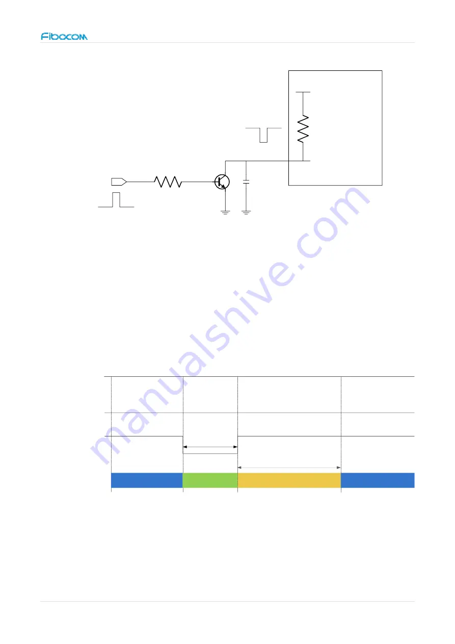
Figure 9. Recommended design for reset circuit
There are two reset control timings as below:
Reset timing 1
st
in Figure 10, PMU of module internal always on in reset sequence,
recommend using in FW upgrade and module recovery;
Reset timing 2
nd
in Figure 11, PMU of module internal will be off in reset sequence
(including whole power off and power on sequence, t
sd
can refer section 3.3.2),
recommend using in system warm boot.
+3.3V
RESET#
Module State
Initialization
Activation
FCPO#
typical TBD
Baseband reset
Activation
t
off1
Figure 10. Reset timing 1st


