


XRD9829REF
7
Rev. 1.00
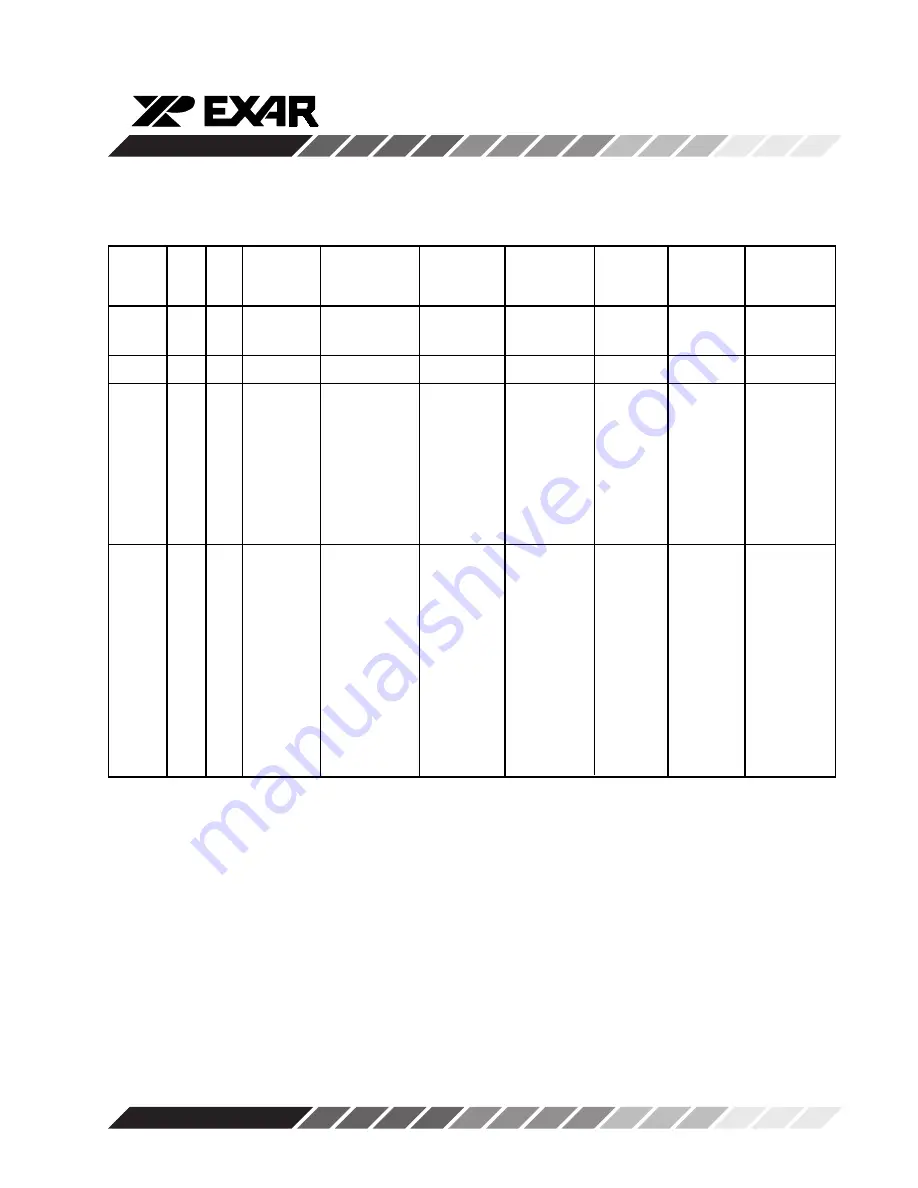
Control Registers
Function
D7
D6
D5
D4
D3
D2
D1
D0
Power-up
(Register
State
S1/S0)
(Note 1)
Gain
(00)
G5
G4
G3
G2
G1
G0
X
X
000000XX
(MSB)
(LSB)
Offset
O7
O6
O5
O4
O3
O2
O1
O0
01000000
(01)
(MSB)
(LSB)
Mode
X
X
V
RT
INPUT DC
DC/AC
CIS/CCD
MUX SEL
MUX SEL
XX000000
(10)
0: INTERNAL
REFERENCE
0: DC
0: CIS
1: EXTERNAL
(V
DCREF
)
1: AC
1: CCD
0:INTERNAL
0 0: VIN0
0 0: VIN0
(V
DCREF
=
0 1: VIN1
0 1: VIN1
AGND)
1 0: VIN2
1 0: VIN2
1: EXTERNAL
1 1: VIN3
1 1: VIN3
(V
DCREF
=V
DCEXT
)
Mode
& Test
(11)
X
X
X
DIGITAL RESET
TEST3
TEST2
TEST1
X
XXX0000X
0: NO RESET
0: TEST3
0: TEST2
0: TEST1
1: RESET
DISABLED
DISABLED
DISABLED
(REGISTERS ARE
1: OUTPUT
1: OUTPUT
1: VIN1 PIN
RESET TO
OF BUFFER
OF PGA
TIED TO
POWER-UP
TIED TO VIN3
TIED TO
INPUT OF
STATES)
PIN (VIN3 PIN
VIN2 PIN
ADC
BECOMES
(VIN2 PIN
(PGA OUTPUT
AN OUTPUT)
BECOMES
DISCONNECTED
AN OUTPUT)
FROM INPUT
OF ADC)
Table 1. Control Register Description for XRD9829
Note:
1
These are the control register settings upon initial power–up. The previous register settings are retained following
a
logic power-down initiated by the PDB signal.
Summary of Contents for XRD9829REF
Page 10: ...XRD9829REF 10 Rev 1 00 Figure 6 Black Target Scan After Global Offset Adjust...
Page 12: ...XRD9829REF 12 Rev 1 00 Figure 8 Black Target Scan After Global and Fine Adjust...
Page 15: ...XRD9829REF 15 Rev 1 00 Figure 11 White Target Scan After Gain Adjustment...
Page 18: ...XRD9829REF 18 Rev 1 00 SchematicsforXRD9829REF Page 1 of 3...
Page 19: ...XRD9829REF 19 Rev 1 00 SchematicsforXRD9829REF Page 2 of 3...
Page 20: ...XRD9829REF 20 Rev 1 00 SchematicsforXRD9829REF Page 3 of 3...
Page 21: ...XRD9829REF 21 Rev 1 00 Notes...
Page 22: ...XRD9829REF 22 Rev 1 00 Notes...
Page 23: ...XRD9829REF 23 Rev 1 00 Notes...


