


Graphics ClientM User Manual
110120-1000A
48
Symbol
Parameter
Min
Typ.
Max
Units
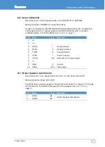
Touch panel
VCC_TSI
Supply voltage
3.3
V
---
A/D sample resolution
10
bit
Notes:
5. Specifications are taken from the Marvell PXA3xx (88AP3xx) Processor Family Electrical,
Mechanical, and Thermal Functional Specification, Doc. No. MV-S105156-00, Rev. 2.0
Version – April 6, 2009.
6. Multi-Function Pin (MFP) drive strength is programmable using the PXA320 Multi-
Function Pin Register (MFPR).
7. Use the MFPR to enable or disable pull-ups.
8. Use the MFPR to enable or disable pull-downs.
9. The PXA320 supports "standard" and "fast" I
2
C speeds of 100 kHz and 400 kHz;
however, the speed is limited to 100 kHz by the RTC chip.
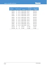
CPLD
A Xilinx XC2C128 CPLD on the GCM provides five GPIOs on header
. For
a description of the GPIOs, see
General-Purpose Inputs and Outputs
Symbol
Parameter
Min
Typ.
Max
Units
GPIO (LVCMOS 1.8V, note 10)
V
CCIO
Input source voltage
1.8
V
V
IH
High-level input voltage (note 11)
0.65V
CCIO
V
CCIO
+ 0.3
V
V
IL
Low-level input voltage
0.35V
CCIO
V
V
OH
High-level output voltage
I
OH
= -8 mA, V
CCIO
= 1.7 V
V
CCIO
– 0.45
V
V
OL
Low-level output voltage
I
OL
= 8 mA, V
CCIO
= 1.7 V
0.45
V
Notes:
10. Specifications are taken from the Xilinx XC2C128 Cool Runner-II CPLD Product
Specification, DS093 (v3.2) March 8, 2007.
11. The V
IH MAX
value is defined by the JEDEC specification for LVCMOS, 1.8V signals. The
CPLD input buffer can tolerate up to 3.9V without physical damage.
Summary of Contents for PXA320
Page 62: ...www eurotech com ...