!
Espressif Systems
ESP8266EX
Hardware User Guide
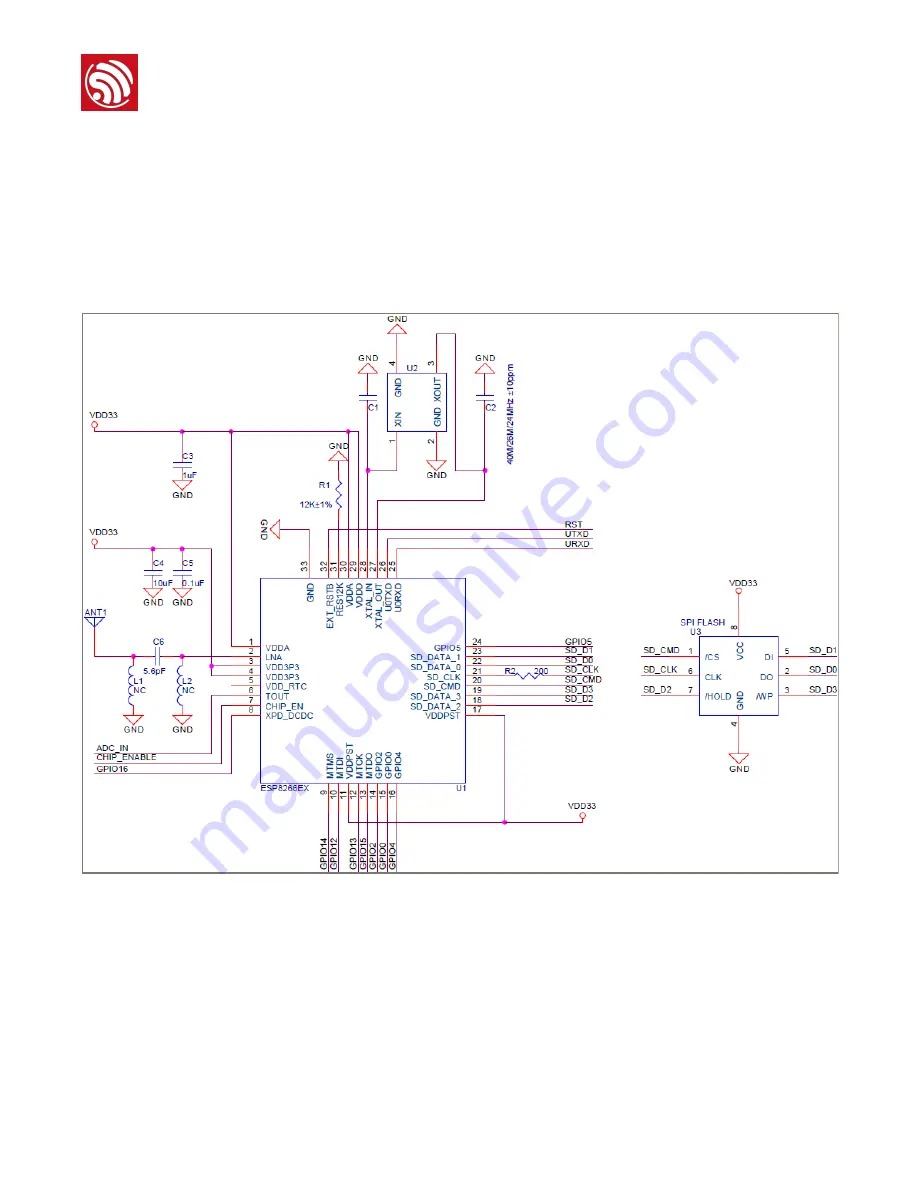
6.3. Schematics of ESP-WROOM Serial WiFi Modules
/
Jun 1, 2015
47 48
Page 1: ...ESP8266EX Hardware User Guide Version 1 1 Espressif Systems IOT Team http bbs espressif com Copyright 2015...
Page 2: ...FICATION OR SAMPLE All liability including liability for infringement of any proprietary rights relating to use of information in this document is disclaimed No licenses express or implied by estoppel...
Page 3: ...17 2 3 1 ESP WROOM Module Design 17 2 3 2 ESP8266EX as Slave Device 20 2 3 3 FAQ On Hardware Design 22 3 ESP LAUNCHER Development Board 24 3 1 Instructions on the Use of ESP LAUNCHER Development Board...
Page 4: ...5 3 Smart light 40 5 4 Smart plug 41 6 Appendix 42 6 1 Schematics of ESP LAUNCHER Development Board 42 Part 1 Interfaces 43 Part 2 5V Power 46 Part 3 Test Board 46 6 2 Schematics of ESP LAUNCHER Test...
Page 5: ...pplication or to offload Wi Fi networking functions from another application processor When ESP8266EX hosts the application it boots up directly from an external flash In has integrated cache to impro...
Page 6: ...d radio co existence features for common cellular Bluetooth DDR LVDS LCD interference mitigation 1 2 Features 802 11 b g n Integrated low power 32 bit MCU Integrated 10 bit ADC Integrated TCP IP proto...
Page 7: ...ramic Chip Hardware Paramaters Peripheral Bus UART SDIO SPI I2C I2S IR Remote Control GPIO PWM Operating Voltage 3 0 3 6V Operating Current Average value 80mA Operating Temperature Range 40 125 Ambien...
Page 8: ...me Appliances Home Automation Smart Plug and lights Mesh Network Industrial Wireless Control Baby Monitors IP Cameras Sensor Networks Wearable Electronics Wi Fi Location aware Devices Security ID Tags...
Page 9: ...iew 2 1 Terminal Configuration and Functions The pin assignments for 32 pin QFN package is illustrated in Fig 2 Figure 2 Pin Assignments Table 2 below presents an overview on the general pin attribute...
Page 10: ...IO12 HSPI_MISO 11 VDDPST P Digital IO Power Supply 1 8V 3 3V 12 MTCK I O GPIO13 HSPI_MOSI UART0_CTS 13 MTDO I O GPIO15 HSPI_CS UART0_RTS 14 GPIO2 I O UART Tx during flash programming GPIO2 15 GPIO0 I...
Page 11: ...O3 26 U0TXD I O UART Tx during flash progamming GPIO1 SPI_CS1 27 XTAL_OUT I O Connect to crystal oscillator output can be used to provide BT clock input 28 XTAL_IN I O Connect to crystal oscillator in...
Page 12: ...ion accuracy and stability of wireless communications High integration level of this chipset tremendously decreases the number of components used in peripheral circuit design Beside ESP8266EX only a n...
Page 13: ...pins is between 1 8V and 3 3V Figure 4 ESP8266EX Digital Power supply Pins Analog Power supply Pins ESP8266EX has 5 analog power supply pins abbreviated as VDD33 in the circuit diagram including Pin...
Page 14: ...supply systems is 3 3V therefore only one rule should be abide by when you power on the device Pin7 CH_EN the power enable pin should be powered on at the same time when or after the power supply syst...
Page 15: ...ngled 2 2 3 Flash Currently the size of flash that we applied in our demo and modules is SPI Flash with 2MB capacity and the package size is SOIC_8 SOP_8 A resistor package size 0402 is connected to P...
Page 16: ...y is 26MHz while the values of C1 and C2 are 10pF C1 C2 22pF if the crystal oscillator frequency is 40MHz Figure 7 ESP8266EX Crystal oscillators Note Defects in the craftsmanship of the crystal oscill...
Page 17: ...uracy is required an accuracy of 12K 1 is recommended Figure 9 External Resistor 2 3 Layout Design PCB layout design of products using chipset ESP8266EX is demonstrated in this part Hereto we mainly f...
Page 18: ...ower supply voltage of those signal lines highlighted in yellow is 3 3V The total width of the power line shall be larger than 15 mil Before the power line reaches the analog power supply pins includi...
Page 19: ...s shall be placed under the four layers of the crystal oscillators The best choice is that no signal lines is placed under the crystal oscillator The TOP layer where is crystal oscillator is placed sh...
Page 20: ...requency should be set near RF lines RF antenna should be set away from high frequency transmitting devices such as crystal oscillators DDR and certain high frequency clocks SDIO_CLK etc Figure 12 ESP...
Page 21: ...length of SDIO lines PCB onboard antenna should not be selected as it receive relatively large interferences and is vulnerable to the coupling noise that might affect RF performance External antenna...
Page 22: ...output signals couple with the input signals due to the cross wiring of input and output signal wires at different layers or high frequency signal wires are wired below the crystal such as the SDIO wi...
Page 23: ...low match of the resistance with the antenna so as to enable the resistance in the section from the chipset RF pin to the antenna to approximate 50 4 Typical phenomenon TX performance is not bad but t...
Page 24: ...66EX development board for quick evaluation and familiarisation of products and for secondary development for customers The size of the demo board is 46mm 78 5mm Functional components on the demo boar...
Page 25: ...of components on the development board is illustrated in Table 3 below Notice For development board provided BEFORE July 1 2015 both of the two Micro USB interfaces should be powered on Among them on...
Page 26: ...n Fig 14 Green light D1 is an indicator light for relay switch control Refer to Part 7 in Fig 14 Blue light D11 and Red light D10 indicate working status of Rx and Tx serial ports respectively Refer t...
Page 27: ...chipset is used as slave device and is connected to the host MCU using the SPI interface that is defined in standard SDIO interface HSPI is connected to Flash2 J3 can be used as chip select of Flash2...
Page 28: ...are altogether 32 pins on the demo board which are illustrated in Figure 15 below Definition of each pin can be found in Table 2 Figure 15 Illustration of Pin Definitions of ESP LAUNCHER Table 4 belo...
Page 29: ...3 and Pin 4 as well as the input voltage of TOUT Pin 6 It can be used in sensors I2C Sensors and display screens with 2 54mm and 1 27mm needles can be connected using I2C interface UART UART0 U0TXD U...
Page 30: ...so as to close HSPI flash Step 5 Pull down the switch that controls GPIO0 so as to enter UART download mode Step 6 Connect with the testing board Step 7 Pull up the 5V power supply switch so as the s...
Page 31: ...na connector The spacing of inserting needles on the test board is 2 54mm which can be easily inserted into breadboard for testing Figure 16 ESP LAUNCHER Test Board 3 3 2 SMD Module ESP WROOM 02 The p...
Page 32: ...ESP8266EX Hardware User Guide Figure 18 Dimensions of ESP WROOM 02 WiIF Module There are altogether 18 pin outs the distribution and definitions of which are listed in Table 5 below Espressif Systems...
Page 33: ...ce the device is powered off the programs in the Memory will be erased However when the programs are burnt into the Flash they will be stored in it and can be invoked and used at any time NO Pin Name...
Page 34: ...using flash downloading tools After burning the programs into Flash pull down IO15 to low voltage level keep IO2 dangled and pull up IO0 to high voltage level The module is then shifted from UART Dow...
Page 35: ...pplied is a SPI flash packed in SOP8 150mil the antenna used is a 1 DBi metal antenna The 2 00mm double pitch applied can be both vertical or straight depending on specific applications Please refer t...
Page 36: ...efer to ESP8266_GCC_LUBUNTU docx on how to set up and configure when the compiling system has been downloaded successfully A Windows sharing folder should also be set up before we run the virtual box...
Page 37: ...SP8266__IOT_SDK_User_Manual on how to compile 1 boot_v1 1 and boot_v1 2 boot_v1 2 is a more compact form of compiling thus more flash space can be saved While boot_v1 3 mainly supports strengthened in...
Page 38: ...MTDO IO15 IO0 IO2 as 0 0 1 after downloading successfully switch to the Flash boot mode 0 1 1 Figure 23 below shows how to use Flash Download Tool Figure 23 Flash Download Tool 4 3 Debugging AT Comma...
Page 39: ...ressif Systems ESP8266EX Hardware User Guide Figure 24 Configuration of UART Serial Port Debugging Tool 2 TCP UDP debugging via the internet Figure 25 TCP UDP Debugging Espressif Systems Jun 1 2015 39...
Page 40: ...ch sensor products will send real time data through I2C interface to ESP8266EX which will upload the data to the server wirelessly When an mobile phone is connected to the public internet it can acces...
Page 41: ...use ordinary GPIO interfaces GPIO interfaces allow control over high and low levels as well as connection and disconnection of relay thus allowing smart control over plug on off This application is ma...
Page 42: ...Espressif Systems ESP8266EX Hardware User Guide 6 Appendix 6 1 Schematics of ESP LAUNCHER Development Board Espressif Systems Jun 1 2015 42 48...
Page 43: ...Espressif Systems ESP8266EX Hardware User Guide Espressif Systems Jun 1 2015 43 48...
Page 44: ...Espressif Systems ESP8266EX Hardware User Guide Part 1 Interfaces Espressif Systems Jun 1 2015 44 48...
Page 45: ...Espressif Systems ESP8266EX Hardware User Guide Espressif Systems Jun 1 2015 45 48...
Page 46: ...Espressif Systems ESP8266EX Hardware User Guide Part 2 5V Power Part 3 Test Board 6 2 Schematics of ESP LAUNCHER Test Board Espressif Systems Jun 1 2015 46 48...
Page 47: ...Espressif Systems ESP8266EX Hardware User Guide 6 3 Schematics of ESP WROOM Serial WiFi Modules Espressif Systems Jun 1 2015 47 48...
Page 48: ...Espressif Systems ESP8266EX Hardware User Guide 6 4 Schematics of ESP8266EX as SDIO SPI Slave Device Espressif Systems Jun 1 2015 48 48...