Edition 080529
-- 11 --
1sC1425
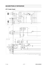
AP1:1 Control circuit
Pressing trigger switch SB1 on the welding torch energises relay RE1 from
control power transformer TR1. The contacts on the relay connect main
transformer TM1 to the mains power supply.
The power supply to RE1 is half--wave rectified by D1. Resistor R1 is
connected in series with the relay and drops the voltage to it. Capacitor C1
(220
µ
F) smoothes the voltage. It also delays the drop--off of relay RE1 by
about 25 ms, to provide a burnback time.
AP1:2 Thermal overload cutout
In the event of a thermal overload, thermal overload cutout ST1 interrupts the
secondary circuit from TR1, causing relay RE1 to drop off and de--energising
the welding circuit. When not operated (i.e. with closed contacts), the cutouts
short--circuit inputs B6 and B7.
Operation of either of the cutouts is indicated by LED V1. Interruption of the
cutout circuit energises the LED via D2, R3 and D3. D2 is a half--wave
rectifier, R3 limits the current through the LED and D3 protects it against
reverse voltage.
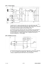
AP1:3 RFI suppression and base load resistors
Capacitors C4 -- C6 protect against RFI. Resistors R12 and R15 provide a
minimum base load for the rectifier bridge: in addition, they act as discharge
resistors for the capacitors.
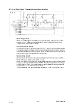
AP1:4 Motor drive circuit
The wire feed motor is powered by the rectified secondary voltage from main
transformer TM1.
Pressing the welding torch trigger switch SB1 provides a supply to thyristor
TY1 via contact B4 from the positive side of the main power rectifier VC1.
Resistors R10 and R14 limit the motor starting current: excessive starting
current would demagnetise the motor. D9 is a squelch diode protecting
against back--emf from the motor.The ignition circuit for TY1 consists of R2,
R4, R5, D5 and C2.
When Q1 is not conducting, operation of the circuit is as follows:
If the voltage at B4 exceeds the motor voltage, C2 charges via R2, R4 and R5.
When the voltage on C2 reaches the trigger voltage (0.5 -- 1.5 V), thyristor TY1
fires. This means that TY1 conducts each half--cycle when Q1 is not
conducting.
D5 protects C2 against negative voltage when Q1 conducts.
Motor voltage control
C3, R11 and potentiometer R13 form a low--pass filter circuit for the motor
supply. R13 picks off a suitable fraction of the motor voltage for connection to
the base of Q1 via diode D6. Q1 starts to conduct at a bases voltage of 0.7 V.
C2 charges more slowly, which means that thyristor TY1 fires later. Motor
voltage is lowest when R13 is in its upper position, the minimum position.
The base voltage is then high and Q1 conducts. The charging time for C2
becomes so long that thyristor TY1 misses some half cycles, firing only (for
example) on every third cycle.
When R13 is in its lower (= maximum) position, the base voltage on Q1 is low
and Q1 does not conduct. In this state, zener diode D7 determines the
maximum motor voltage.
Summary of Contents for Origo Mag C171
Page 8: ...Edition 080529 8 1sC1425 Mig C141 ...
Page 9: ...Edition 080529 9 1sC1425 Mig C151 ...
Page 10: ...Edition 080529 10 1sC1425 DESCRIPTION OF OPERATION AP1 Control board clka0e02 ...
Page 12: ...Edition 080529 12 1sC1425 AP1 Mig C141 C151 component positions clka0e03 ...
Page 15: ...Edition 080529 15 1sC1425 Mag C171 ...
Page 16: ...Edition 080529 16 1sC1425 Mag C201 ...
Page 17: ...Edition 080529 17 1sC1425 DESCRIPTION OF OPERATION AP1 Control board clka1e03 ...
Page 18: ...Edition 080529 18 1sC1425 clka1e04 ...
Page 23: ...Edition 080529 23 1sC1425 AP1 Mag C171 C201 component positions clka1e05 ...
Page 26: ...Edition 080529 26 1sC1425 Mag C251 ...
Page 31: ...Edition 080529 clkb0e13 31 1sC1425 AP1 Mag C251 component positions ...
Page 36: ...Edition 080529 36 2sC1425 OrigoTM Mig C151 1 3 2 ...
Page 37: ...Edition 080529 37 2sC1425 OrigoTM Mag C171 C201 C251 1 3 2 Electrical installation ...
Page 43: ... 43 notes NOTES ...
Page 44: ... 44 notes ...


