background image

LCD Interface Pin Mapping

S5U13706B00C Rev. 1.0 Evaluation Board

Seiko Epson Corporation

17

Rev. 5.1

Note

1

 When dip switch SW1-4 is open (CNF3 = 0 at RESET#), GPIO[6:0] are at low output

states after reset. If REG[10h] bits[1:0] are set for either HR-TFT or D-TFD, some of
the pins are used for the HR-TFT or D-TFD interfaces and are not available as GPIO
pins.

Table 5-2: Extended LCD Signal Connector (H2)

Pin 

Name

Connector 

Pin No.

Monochrome 

Passive Panel

Color Passive Panel

Color TFT Panel

 Single

Single

Others

HR-

TFT

1

D-TFD

1

Format 1 Format 2

4-bit

8-bit

4-bit

8-bit

8-bit

16-Bit

9-bit

12-bit

18-bit

18-bit

18-bit

GPIO0

1

GPIO0

PS

XINH

GPIO1

3

GPIO1

CLS

YSCL

GPIO2

5

GPIO2

REV

FR

GPIO3

7

GPIO3

SPL

FRS

GPIO4

9

GPIO4

GPIO4

RES

GPIO5

11

GPIO5

GPIO5

DD_P1

GPIO6

13

GPIO6

GPIO6

YSCLD

CVOUT

15

CVOUT

GND

2, 4, 6, 8, 10, 

12, 14, 16

GND

Summary of Contents for S5U13706B00C

Page 1: ...Rev 5 1 S1D13706 Embedded Memory LCD Controller S5U13706B00C Rev 1 0 Evaluation Board User Manual Document Number X31B G 004 05 1 ...

Page 2: ... export and or to otherwise dispose of the products and any technical information furnished if any for the devel opment and or manufacture of weapon of mass destruction or for other military purposes All brands or product names mentioned herein are trademarks and or registered trademarks of their respective companies SEIKO EPSON CORPORATION 2001 2018 All rights reserved Evaluation Board Kit and De...

Page 3: ... PCI Bus Support 18 6 2 Direct Host Bus Interface Support 18 6 3 S1D13706 Embedded Memory 18 6 4 Manual Software Adjustable LCD Panel Positive Power Supply VDDH 18 6 5 Manual Software Adjustable LCD Panel Negative Power Supply VLCD 19 6 6 Software Adjustable LCD Backlight Intensity Support Using PWM 20 6 7 Passive Active LCD Panel Support 20 6 7 1 Buffered LCD Connector 20 6 7 2 Extended LCD Conne...

Page 4: ...4 Seiko Epson Corporation S5U13706B00C Rev 1 0 Evaluation Board Rev 5 1 THIS PAGE LEFT BLANK ...

Page 5: ...d The board is designed as an evaluation platform for the S1D13706 Embedded Memory LCD Controller This document is updated as appropriate Please check for the latest revision of this document before beginning any development The latest revision can be downloaded at vdc epson com We appreciate your comments on our documentation Please contact us via email at vdc documentation ea epson com ...

Page 6: ...ble negative LCD bias power supply from 24V to 8V Software adjustable backlight intensity support 4 8 bit 3 3V or 5V single monochrome passive LCD panel support 4 8 16 bit 3 3V or 5V single color passive LCD panel support 9 12 18 bit 3 3V or 5V active matrix TFT LCD panel support Direct interface for 18 bit Epson D TFD LCD panel support Direct interface for 18 bit Sharp HR TFT LCD panel support Pr...

Page 7: ...low both evaluation board and S1D13706 LCD controller to be configured for a specified evaluation platform 3 1 Configuration DIP Switches The S1D13706 has configuration inputs CNF 7 0 which are read on the rising edge of RESET In order to configure the S1D13706 for multiple Host Bus Interfaces a ten position DIP switch S1 is required The following figure shows the location of DIP switch SW1 on the...

Page 8: ...on DIP Switch Settings Switch S1D13706 Signal Value on this pin at rising edge of RESET is used to configure Closed On 1 Open Off 0 SW1 3 1 CNF 2 0 Select host bus interface as follows CNF2 CNF1 CNF0 Host Bus Interface 0 0 0 SH 4 SH 3 0 0 1 MC68K 1 0 1 0 MC68K 2 0 1 1 Generic 1 1 0 0 Generic 2 1 0 1 RedCap 2 1 1 0 DragonBall 1 1 1 Reserved Note The host bus interface is 16 bit SW1 4 CNF3 Enable GP...

Page 9: ...Specification document number X28B A 001 xx for details Note When configured for Sharp HR TFT or Epson D TFD panels JP1 must be set to no jumper and JP6 must be set to position 2 3 Figure 3 2 Configuration Jumper JP1 Location Table 3 2 Jumper Summary Jumper Function Position 1 2 Position 2 3 No Jumper JP1 GPIO0 Connection GPIO0 connected to SW1 9 for hardware video invert GPIO0 disconnected from S...

Page 10: ...tting Position 2 3 sets the CLKI2 source to the external oscillator at U5 Figure 3 3 Configuration Jumper JP2 Location JP3 CLKI Source JP2 selects the source for the CLKI Position 1 2 sets the CLKI2 source to VCLKOUT from the Cypress clock synthesizer default setting Position 2 3 sets the CLKI2 source to the external oscillator at U6 Figure 3 4 Configuration Jumper JP3 Location JP2 MCLKOUT Externa...

Page 11: ...nverts the GPO signal before sending it to H1 Figure 3 5 Configuration Jumper JP4 Location JP5 Contrast adjust for ve LCD bias VDDH JP5 selects the type of control used for contrast adjustment of the ve LCD bias VDDH Position 1 2 selects software control of the contrast adjustment Position 2 3 selects manual control of the contrast adjustment using potentiometer R24 default setting Figure 3 6 Conf...

Page 12: ...pson D TFD panels JP1 must be set to no jumper and JP6 must be set to position 2 3 Figure 3 7 Configuration Jumper JP6 Location JP7 Contrast adjust for ve LCD bias VLCD JP7 selects the type of control used for contrast adjustment of the ve LCD bias VLCD Position 1 2 selects software control of the contrast adjustment Position 2 3 selects manual control of the contrast adjustment using potentiomete...

Page 13: ...1 Generic 2 Hitachi SH 3 SH 4 Motorola MC68K 1 Motorola MC68K 2 Motorola REDCAP2 Motorola MC68EZ328 MC68VZ328 DragonBall AB 16 1 A 16 1 A 16 1 A 16 1 A 16 1 A 16 1 A 16 1 A 16 1 AB0 A01 A0 A01 LDS A0 A01 A01 DB 15 0 D 15 0 D 15 0 D 15 0 D 15 0 D 15 0 2 D 15 0 D 15 0 CS External Decode CSn External Decode CSn CSA M R External Decode CLKI BUSCLK BUSCLK CKIO CLK CLK CLK CLK BS Connected to VDD 3 BS A...

Page 14: ...to DB7 of the S1D13706 11 Ground 12 Ground 13 Connected to DB8 of the S1D13706 14 Connected to DB9 of the S1D13706 15 Connected to DB10 of the S1D13706 16 Connected to DB11 of the S1D13706 17 Ground 18 Ground 19 Connected to DB12 of the S1D13706 20 Connected to DB13 of the S1D13706 21 Connected to DB14 of the S1D13706 22 Connected to DB15 of the S1D13706 23 Connected to RESET of the S1D13706 24 Gr...

Page 15: ... Ground 11 Connected to A8 of the S1D13706 12 Connected to A9 of the S1D13706 13 Connected to A10 of the S1D13706 14 Connected to A11 of the S1D13706 15 Connected to A12 of the S1D13706 16 Connected to A13 of the S1D13706 17 Ground 18 Ground 19 Connected to A14 of the S1D13706 20 Connected to A15 of the S1D13706 21 Connected to A16 of the S1D13706 22 Not connected 23 Not connected 24 Not connected...

Page 16: ...R2 1 D8 B5 1 G1 G2 G4 G4 G4 FPDAT5 11 D1 D5 D1 B1 1 D5 G2 1 D5 B1 1 D9 R5 1 G0 G1 G3 G3 G3 FPDAT6 13 D2 D6 D2 G1 1 D6 B1 1 D6 G1 1 D10 G4 1 B2 B3 B5 B5 B5 FPDAT7 15 D3 D7 D3 R1 1 D7 R1 1 D7 R1 1 D11 B3 1 B1 B2 B4 B4 B4 FPDAT8 17 driven 0 driven 0 driven 0 driven 0 driven 0 D4 G3 1 B0 B1 B3 B3 B3 FPDAT9 19 driven 0 driven 0 driven 0 driven 0 driven 0 D5 B2 1 driven 0 R0 R2 R2 R2 FPDAT10 21 driven 0...

Page 17: ...terfaces and are not available as GPIO pins Table 5 2 Extended LCD Signal Connector H2 Pin Name Connector Pin No Monochrome Passive Panel Color Passive Panel Color TFT Panel Single Single Others HR TFT1 D TFD1 Format 1 Format 2 4 bit 8 bit 4 bit 8 bit 8 bit 16 Bit 9 bit 12 bit 18 bit 18 bit 18 bit GPIO0 1 GPIO0 PS XINH GPIO1 3 GPIO1 CLS YSCL GPIO2 5 GPIO2 REV FR GPIO3 7 GPIO3 SPL FRS GPIO4 9 GPIO4...

Page 18: ...ytes of embedded SRAM The 80K byte display buffer address space is directly and contiguously available through the 17 bit address bus 6 4 Manual Software Adjustable LCD Panel Positive Power Supply VDDH Most passive LCD color and passive single monochrome LCD panels require a positive bias voltage between 24V and 40V The S5U13706B00C uses a Maxim MAX754 LCD Contrast Controller to provide this volta...

Page 19: ...oftware to provide an output voltage from 8V to 24V CVOUT and GPO of the S1D13706 are connected to ADJ and CTRL of MAX749 The output voltage VLCD can be adjusted from 8V to 24V in 64 steps by sending pulses to CVOUT Each CVOUT pulse increments VLCD one step towards 24V When decremented beyond 24V VLCD resets to 8V again In other words 63 pulses equal incrementing 1 step After the MAX749 is reset s...

Page 20: ...vided on the 40 pin LCD connector H1 For connection information refer to Table 5 1 LCD Signal Connector H1 on page 16 6 7 1 Buffered LCD Connector The buffered LCD connector H1 provides the same LCD panel signals as those directly from S1D13706 but with voltage adapting buffers selectable to 3 3V or 5 0V Pin 32 on this connector provides a voltage level of 3 3V or 5 0V to the LCD panel logic see J...

Page 21: ... and CLKI2 Jumpers JP2 and JP3 allow selection of external oscillators U5 and U6 as the clock source for both CLKI and CLKI2 For further information see Table 3 2 Jumper Summary on page 9 7 1 Clock Programming The S1D13706 utilities automatically program the clock generator If manual programming of the clock generator is required refer to the source code for the S1D13706 utilities available on the...

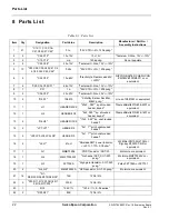
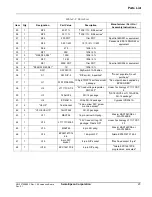
Page 22: ...F pckg Lite on 1N5819M or equivalent 11 1 H1 HEADER 20X2 20x2 025 sq shrouded header keyed Thomas Betts P N 636 4207 or equivalent 12 1 H2 HEADER 8X2 8x2 025 sq shrouded header keyed Thomas Betts P N 636 1607 or equivalent 13 2 H4 H3 HEADER 17X2 17x2 025 sq unshrouded header 14 2 JP7 JP1 HEADER 2 2x1 1 pitch unshrouded header 15 5 JP2 JP3 JP4 JP5 JP6 HEADER 3 3x1 1 pitch unshrouded header 16 2 L2 ...

Page 23: ...d by EPSON R D 38 1 U2 LT1117CST 5 5V fixed voltage regulator SOT 223 Linear Technology LT1117CST 5 39 1 U3 74AHC04 SO 14 package NS 74VHC04 or TI 74AHC04 SO 14 package 40 1 U4 ICD2061A Wide SO 16 package Cypress ICD2061A 41 2 U6 U5 Test Socket 14 pin narrow DIP screw machine socket 42 4 U7 U8 U9 U10 74HCT244 SO 20 package 43 1 U11 MAX754 16 pin narrow SO pckg Maxim MAX754CSE or MAX754ESE 44 1 U12...

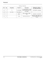
Page 24: ...Crystal HC49 Low Profile pckg FOXS 143 20 or equivalent 50 7 JP1 JP7 Micro Shunt 51 1 Bracket Computer Bracket Blank PCI Keystone Cat No 9203 52 2 Screw Pan head 4 40 x 1 4 Screw pan head 4 40 x 1 4 please assemble bracket onto board Table 8 1 Parts List Item Qty Designation Part Value Description Manufacturer Part No Assembly Instructions ...

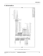
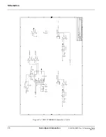
Page 25: ...1 S1D13706F00A 5 4 3 2 99 98 97 96 95 94 93 92 91 90 89 88 87 35 34 33 32 31 30 29 28 27 24 23 22 21 20 19 18 15 77 6 7 8 9 10 11 12 13 17 85 84 83 82 81 80 79 78 55 56 57 58 59 60 61 64 65 66 67 68 69 70 71 72 73 74 52 53 54 48 46 38 47 45 44 43 42 41 40 39 86 14 25 36 50 62 75 100 16 26 37 49 63 76 1 51 AB0 AB1 AB2 AB3 AB4 AB5 AB6 AB7 AB8 AB9 AB10 AB11 AB12 AB13 AB14 AB15 AB16 DB0 DB1 DB2 DB3 DB...

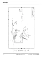
Page 26: ...SCLK 1 5 6 5V 5V 12V 5V 5V 3 3V 3 3V 3 3V 3 3V 3 3V 3 3V JP3 HEADER 3 1 2 3 JP2 HEADER 3 1 2 3 C9 0 1u U6 Test Socket 1 8 7 14 NC OUT GND VCC U3F 74AHC04 13 12 14 7 C16 0 1u U5 Test Socket 1 8 7 14 NC OUT GND VCC C17 0 1u U2 LT1117CST 5 3 1 2 VIN ADJ VOUT C13 0 1u C10 0 1u C11 0 1u C12 10u 10V U4 ICD2061A 13 3 5 1 2 12 14 16 4 6 7 11 15 8 9 10 VDD AVDD GND S0 CLK S1 DATA INIT0 INIT1 PWRDWN OE XTAL...

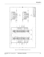
Page 27: ...VOUT 1 4 GPIO4 1 GPIO5 1 2 GPIO2 1 GPIO1 1 GPIO6 1 2 GPIO0 1 GPO 1 4 PWMOUT 1 FPSHIFT 1 DRDY 1 FPFRAME 1 FPLINE 1 LCDVCC LCDVCC LCDVCC 12V LCDVCC LCDVCC 3 3V C19 0 1u H1 HEADER 20X2 1 2 3 4 5 6 7 8 9 10 11 12 13 14 15 16 17 18 19 20 21 22 23 24 25 26 27 28 29 30 31 32 33 34 35 36 37 38 39 40 U7 74HCT244 2 4 6 8 11 13 15 17 1 19 18 16 14 12 9 7 5 3 20 10 1A1 1A2 1A3 1A4 2A1 2A2 2A3 2A4 1G 2G 1Y1 1Y...

Page 28: ...8 V ADJ CTRL FB GND DLOW DHI CS C29 0 1u L2 47uH R26 470 C30 68u 10V Q4 MMBT2222A D2 1N5819 1 2 R28 100K C26 10u 10V C25 0 1u Q2 MMFT3055VL 1 2 3 4 R27 22K R25 0 22 1 4W R30 1 2M Q1 MMBT3906L 3 1 2 C24 10u 63V C22 22u 10V R31 500K POT 1 3 2 R29 100K C27 0 1u R20 80K U12 LT1117CM 3 3 3 1 2 VIN ADJ VOUT JP7 HEADER 2 1 2 D1 1N5819 1 2 R23 301 1 C31 1n C32 10u 63V R22 402 1 C28 22u 10V C23 0 22u JP6 H...

Page 29: ...1 PCI B 1 2 3 4 5 6 7 8 9 10 11 14 15 16 17 18 19 20 21 22 23 24 25 26 27 28 29 30 31 32 33 34 35 36 37 38 39 40 41 42 43 44 45 46 47 48 49 52 53 54 55 56 57 58 59 60 61 62 12V TCK GND TDO 5V 5V INTB INTD PRSNT 1 RESERVED PRSNT 2 RESERVED GND CLK GND REQ VI O AD31 AD29 GND AD27 AD25 3 3V C BE3 AD23 GND AD21 AD19 3 3V AD17 C BE2 GND IRDY 3 3V DEVSEL GND LOCK PERR 3 3V SERR 3 3V C BE1 AD14 GND AD12 ...

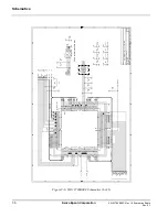
Page 30: ...7 48 49 50 51 52 53 54 55 56 57 58 59 60 61 62 63 64 65 66 67 68 69 70 71 72 73 74 75 76 77 78 79 80 81 82 83 84 85 86 87 88 89 90 91 92 93 94 95 96 97 98 99 100 101 102 103 104 105 106 107 108 109 110 111 112 113 114 115 116 117 118 119 120 121 122 123 124 125 126 127 128 129 130 131 132 133 134 135 136 137 138 139 140 141 142 143 144 IO1 IO2 IO3 nCE GND Vccint Vccio IO8 IO9 IO10 IO11 IO12 IO13 I...

Page 31: ...Board Layout S5U13706B00C Rev 1 0 Evaluation Board Seiko Epson Corporation 31 Rev 5 1 10 Board Layout Figure 10 1 S5U13706B00C Board Layout ...

Page 32: ... Epson Corporation S5U13706B00C Rev 1 0 Evaluation Board Rev 5 1 11 Change Record X31A G 004 05 Revision 1 2 Issued April 09 2018 Updated address contact page Updated Epson web page and email address Minor formatting changes ...

Page 33: ... more information on Epson Display Controllers visit the Epson Global website https global epson com products_and_drivers semicon products display_controllers For Sales and Technical Support contact the Epson representative for your region https global epson com products_and_drivers semicon information support html ...

Reviews: