S1F76610 Series
S1F70000 Series
EPSON
2–13
Technical Manual
S1F76610
Series
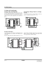
Serial Connection
Connecting two or more chips in series obtains a higher
output voltage than can be obtained using a parallel
<Precautions when connecting loads>
In case of series connections, when connecting loads
between the first stage V
DD
(or other potential of the
second stage V
DD
or up) and the second stage V
REG
as
shown in Fig. 2-13, be cautions about the following
point.
* When normal output is not occurring at the V
REG
ter-
minal such as at times of starting up or when turning
the V
REG
off by P
OFF
signals, if current flows into the
second stage V
REG
terminal through the load from
connection, however, this also raises the output imped-
ance.
the first stage V
DD
(or other potential of the second
stage V
DD
or up) to cause a voltage exceeding the
absolute maximum rating for the second stage V
DD
at
the V
REG
terminal, normal operation of the IC may be
hampered. Consequently, When making a series
connection, insert a diode D1 between the second
stage V
I
and V
REG
as shown in Fig. 2-13 so that a
voltage exceeding the second stage V
DD
or up may
not be applied to the V
REG
terminal.
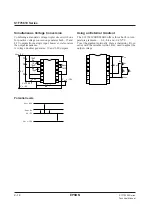
Positive Voltage Conversion
Adding diodes converts a negative voltage to a positive
one.
To convert the voltage tripler shown earlier to a voltage
doubler, remove C2 and D2, and short circuit D3. Small
Schottky diodes are recommended for all these diodes.
The resulting voltage is lowered by V
F
, the voltage drop
in the forward direction for each diode used. For ex-
ample, if V
DD
= 0V, V
I
= –5V, and V
F
= 0.6V, the re-
sulting voltages would be as follows.
• For a voltage tripler,
V
O
= 10 – (3
×
0.6) = 8.2V
• For a voltage doubler,
V
O
= 5 – (2
×
0.6) = 3.8V
10
µ
F
1M
Ω
10
µ
F
10
µ
F
+
–
+
–
V
DD
= 0V
V
O
= –20V
V
REG
'
= –15V
V
DD
'
= V
I
= –5V
D1
V
I
= –5V
5V
+
–
10
µ
F
+
–
+
1
2
3
4
5
6
7
14
13
12
11
10
9
8
1
2
3
4
5
6
7
14
13
12
11
10
9
8
10
µ
F
+
–
10
µ
F
100k
Ω
1M
Ω
to
–
Load
V
O
= –10V= V
I
V
I
= –5 V
V
DD
= 0 V
V
O
= 8.2 V
C3
10
µ
F
+
C2
10
µ
F
+
C1
10
µ
F
+
R
OSC
1 M
Ω
D1
D2
5 V
D3
1
2
3
4
5
6
7
14
13
12
11
10
9
8

