background image

S1F76610 Series

2–10

EPSON

S1F70000 Series

Technical Manual

0

5

10

15

20

0.30

0.25

0.20

0.15

0.10

0.05

0.00

Ta = 25

°

C

V

O

 = –5V

V

O

 = –10V

V

O

 = –15V

I

O

 [mA]

|V

REG

-V

O

| [V]

50

0

–50

–40

–20

0

20

40

60

80

100

CT0

Ta [

°

C]

100

×

|V

REG

(

°

C)|-|V

REG

(25

°

C)|/|V

REG

(25

°

C)| [%]

CT1

CT2

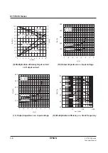
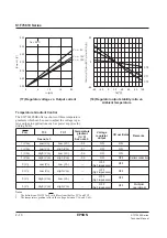
(17) Regulator voltage vs. Output current

(18) Regulator output stability ratio vs.

Ambient temperature

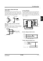
Temperature Gradient Control

The S1F7661C0B0 offers a choice of three temperature
gradients which can be used to adjust the voltage regu-
lator output in applications such as power supplies for
driving LCDs.

Notes
1.

The definition of LOW for P

OFF

 differs from that for TC1 and TC2.

2.

The temperature gradient affects the voltage between V

DD

 and V

REG

.

P

OFF

1 (V

DD

)

1 (V

DD

)

1 (V

DD

)

1 (V

DD

)

0 (V

I

)

0 (V

I

)

0 (V

I

)

0 (V

I

)

TC2

See note 1.

Low (V

O

)

Low (V

O

)

High (V

DD

)

High (V

DD

)

Low (V

O

)

Low (V

O

)

High (V

DD

)

High (V

DD

)

TC1

Low (V

O

)

High (V

DD

)

Low (V

O

)

High (V

DD

)

Low (V

O

)

High (V

DD

)

Low (V

O

)

High (V

DD

)

–0.4

–0.1

–0.6

–0.6

Temperature

gradient

(%/˚C)

See note 2.

Voltage

regulator

output

CR osciliator

Remarks

ON

ON

ON

ON

OFF

(high impedance)

OFF

(high impedance)

OFF

(high impedance)

OFF

(high impedance)

ON

ON

ON

OFF

OFF

OFF

OFF

OFF

Serial connection

Multiplier

operational

Summary of Contents for S1F76610 series

Page 1: ...0 Series EPSON Electronic Devices Website ELECTRONIC DEVICES MARKETING DIVISION First issue November 1990 U Revised July 2001 in Japan H B 4 5mm POWER SUPPLY IC S1F76610 Technical Manual http www epson co jp device This manual was made with recycle paper and printed using soy based inks ...

Page 2: ...0 4 and 0 6 C VDD Voltage multiplier 1 Voltage multiplier 2 CR oscilator Reference voltge generator Temperature gradient selector Voltage regulator TC1 TC2 RV POFF VREG VO VI OSC2 OSC1 CAP1 CAP1 CAP2 CAP2 Multiplication stage Stabilization stage BLOCK DIAGRAM S1F76610 Series CMOS DC DC Converter Voltage Doubler Tripler Voltage Regulator External shut down control 2µA maximum output current when sh...

Page 3: ...ier Negative charge pump connection for 2 multiplier Positive charge pump connection for 3 multiplier Negative charge pump connection for 3 multiplier or 2 multiplier output Pin No 1 2 3 4 5 6 7 8 9 10 11 12 13 14 Pin name CAP1 CAP1 CAP2 CAP2 TC1 TC2 VI VO VREG RV POFF OSC2 OSC1 VDD Temperature gradient selects Negative supply system ground 3 multiplier output Voltage regulator output Voltage regu...

Page 4: ...d 2 2V is shown in the following figure Note that diode D1 should have a maximum forward voltage of 0 6V with 1 0mA forward current 2 RL min can be varied depending on the input voltage Rating Parameter Symbol Conditions Oscillator startup voltage Oscillator shutdown voltage Load resistance Output current Clock frequency CR oscillator network resistance Capacitance Stabilization voltage sensing re...

Page 5: ...oad resistance kΩ 6 5 4 3 2 1 5 VSTA2 VSTA1 Voltage tripler Voltage doubler Symbol Parameter Conditions Input voltage Output voltage Regulator voltage Stabilization circuit operating voltage Multiplier current Stabilization current Quiescent current Clock frequency VI VO VREG VO IOPR1 IOPR2 IQ fOSC RL RRV 1MΩ VO 18V RL ROSC 1MΩ RL RRV 1MΩ VO 15V TC2 TC1 VO RL ROSC 1MΩ Rating Min 6 0 18 0 18 0 18 0...

Page 6: ...ient POFF TC1 TC2 OSC1 and RV input leakage current Symbol RO Peff RSAT VRV CT ILKI VREG IO Conditions IO 10mA IO 5mA VREG VO VREG VO 18 to 8V VREG 8V RL Ta 25 C VO 15V VREG 8V Ta 25 C IO 0 to 10µA TC1 VDD TC2 VO RSAT VREG VO IO IO 0 to 10µA RV VDD Ta 25 C TC2 TC1 VO Ta 25 C TC2 VDD TC1 VO Ta 25 C See note Rating Min 90 0 2 3 1 7 1 1 0 25 0 5 0 7 Typ 150 95 0 0 2 5 0 8 0 1 5 1 3 0 9 0 1 0 4 0 6 Ma...

Page 7: ...6 15 14 13 12 11 10 9 8 40 20 0 20 40 60 80 100 Ta C f OSC kHz VI 5 0V VI 3 0V VI 2 0V 1 Clock frequency vs External resistance 2 Clock frequency vs Ambient temperature 150 100 50 0 7 6 5 4 3 2 1 0 VI V I OPR µA fOSC 40kHz fOSC 20kHz fOSC 10kHz Ta 25 C 0 5 10 15 0 10 20 30 40 IO mA V O V Ta 25 C VI 5 0V 2 multiplier 3 multiplier 3 Multiplier current vs Input voltage 4 Output voltage vs Output curr...

Page 8: ...ut current 100 90 80 70 60 50 40 30 20 10 0 100 90 80 70 60 50 40 30 20 10 0 0 10 20 30 40 50 IO mA I I mA Peff 3 multiplier II Ta 25 C VI 5 0V 2 multiplier Peff 3 multiplier Peff 2 multiplier II 0 5 10 15 20 25 30 IO mA 60 54 48 42 36 30 24 18 12 6 0 I I mA 100 90 80 70 60 50 40 30 20 10 0 Peff Ta 25 C VI 3 0V 3 multiplier II 3 multiplier Peff 2 multiplier Peff 2 multiplier II 7 Multiplication ef...

Page 9: ... 300 200 100 0 7 6 5 4 3 2 1 0 VI V R O Ω Ta 25 C IO 6mA 3 multiplier 2 multiplier 9 Multiplication efficiency input current 10 Output impedance vs Input voltage vs Output current 7 6 5 4 3 2 1 0 VI V 500 400 300 200 100 0 R O Ω 3 multiplier Ta 25 C IO 10mA 2 multiplier 100 90 80 70 60 50 1 10 100 1000 fOSC kHz Peff IO 2mA IO 5mA IO 10mA IO 20mA IO 30mA Ta 25 C VI 5 0V 11 Output impedance vs Input...

Page 10: ...850 7 900 7 950 8 000 0 0001 0 0010 0 0100 0 1000 Ta 25 C V REG V IO V 13 Multiplication efficiency vs Clock frequency 14 Output voltage vs Output current 5 850 5 900 5 950 6 000 0 0001 0 0010 0 0100 0 1000 V REG V IO V VO 9V Ta 25 C 2 850 2 900 2 950 3 000 V REG V 0 0001 0 0010 0 0100 0 1000 IO V VO 6V Ta 25 C 15 Output voltage vs Output current 16 Output voltage vs Output current ...

Page 11: ...e regu lator output in applications such as power supplies for driving LCDs Notes 1 The definition of LOW for POFF differs from that for TC1 and TC2 2 The temperature gradient affects the voltage between VDD and VREG POFF 1 VDD 1 VDD 1 VDD 1 VDD 0 VI 0 VI 0 VI 0 VI TC2 See note 1 Low VO Low VO High VDD High VDD Low VO Low VO High VDD High VDD TC1 Low VO High VDD Low VO High VDD Low VO High VDD Low...

Page 12: ...ies a reference voltage to the voltage regulator to control the output This voltage can be switched ON and OFF VDD VREG RRV 100 kΩ to 1 MΩ RV POFF Control signal Voltage Multiplier The voltage multiplier uses the clock signal from the oscillator to double or triple the input voltage This re quires three external capacitors two charge pump ca pacitors between CAP1 and CAP1 and CAP2 and CAP2 respect...

Page 13: ...e Doubler To convert this curcuit to a voltage doubler remove ca pacitor C2 and short circuit CAP2 to VO VI 5 V ROSC 1 MΩ C1 10µF C2 5V 10µF C3 10 µF VO 15 V VDD 0 V 14 13 12 11 10 9 8 1 2 3 4 5 6 7 Parallel Connection Connecting two or more chips in parallel reduces the output impedance by 1 n where n is the number of de vices used Only the single output smoothing capacitor C3 is re VDD 0 V VI 5 ...

Page 14: ...t the VREG terminal normal operation of the IC may be hampered Consequently When making a series connection insert a diode D1 between the second stage VI and VREG as shown in Fig 2 13 so that a voltage exceeding the second stage VDD or up may not be applied to the VREG terminal Positive Voltage Conversion Adding diodes converts a negative voltage to a positive one To convert the voltage tripler sh...

Page 15: ...rates 10 and 3 8V outputs Potential levels VDD 0 V VI 5 V VO1 15 V VO2 8 2V Using an External Gradient The S1F7661C0B0 M0B0 offers three built in tem perature gradients 0 1 0 4 and 0 6 C To set the gradient externally place a thermistor RT in series with the variable resistor RRV used to adjust the output voltage RT VREG RRV R1 10 µF VDD RP 1 2 3 4 5 6 7 14 13 12 11 10 9 8 VDD 0 V VI 5 V VO2 8 2 V...

Reviews: