RX8111CE
Page
−
58
ETM61E-01
14.10.4. Slave address
The I
2
C-Bus devices do not have any chip select or chip enable pins. All I
2
C-Bus devices are memorized with a fixed unique
number in it. The chip selection on the I
2
C-Bus is executed, when the interface starts, the master device sends the required slave
address to all devices on the I
2
C-Bus. The receiving device only reacts for interfacing, when the required slave address is agreed
with its own slave address.
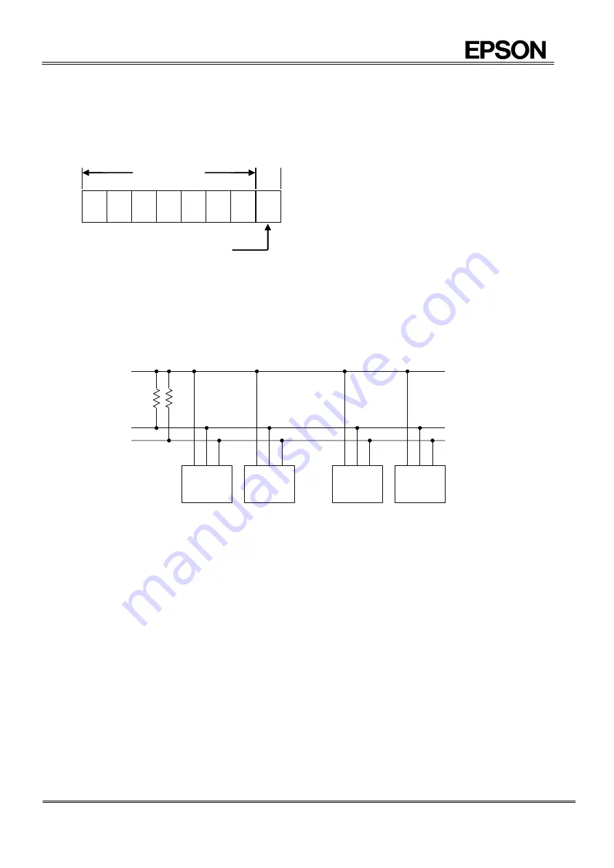
During in actual data transmission, the transmitted data contains the slave address and the data with R/W
(read/write) bit.
Slave address
R/W
bit
bit 7
bit 6
bit 5
bit 4
bit 3
bit 2
bit 1
bit 0
0
1
1
0
0
1
0
R/W
0 when write mode
1 when read mode
14.10.5. System configuration
All ports connected to the I
2
C-Bus must be either open drain or open collector ports in order to enable AND connections to multiple
devices.
SCL and SDA are both connected to the VIO line via a pull-up resistance. Consequently, SCL and SDA are both held at high level
when the Bus is released (when communication is not being performed).
Master
Transmitter/
Receiver
Slave
Transmitter/
Receiver
Other I
2
C bus device
CPU, etc.
RX8111CE
SDA
SCL
V
IO
Master
Transmitter/
Receiver
Slave
Transmitter/
Receiver
Figure 49 I
2
C-Bus connection
Any device that controls the data transmission and data reception is defined as a "Master".
and any device that is controlled by a master device is defined as a “Slave”.
The device transmitting data is defined as a “Transmitter” and the device receiving data is defined as a receiver”
In the case of this RTC module, controllers such as a CPU are defined as master devices and the RTC module is defined as a
slave device. When a device is used for both transmitting and receiving data, it is defined as either a transmitter or receiver
depending on these conditions.


