Enclustra MA-PM3-C-R3 User Manual Download Page 32


23/04/2019 

32 / 43 

Version 1.09 

3.0 controller includes a 32 Bit ARM926 core operating at 200 MHz using a 19.2 MHz crystal oscillator. 
It can access the I

2

C bus, SPI flash of the FPGA and exchange debug or control information with the 

USB 2.0 UART controller over UART. A JTAG interface is available on connector J801 to debug and 
download the application. 

By default, the PMODE pins of the FX3 are configured for SPI boot with USB fall back (refer to Table 
25)
. Hence, the application code can be stored in a dedicated 16 Mbit SPI flash that is read during 
startup. If no valid boot image is found, the FX3 tries to load the application from USB. By removing 
R301 and assembling 10 k to R300, the boot mode can be set to USB boot only. 

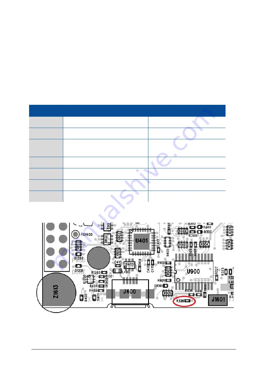
To temporarily prevent the FX3 to boot from the SPI flash R326 can be short circuited. The location of 
R326 is shown in Figure 8. 

PMODE[2:0] 

Boot from 

Comments 

F00 

Sync ADMUX (16 Bit) 

Not selectable 

F01 

Async ADMUX (16 Bit) 

Not selectable 

F11 

USB boot 

Remove R301 and assemble 10 k to 
R300 

F0F 

Async RAM (16 Bit) 

Not selectable


F1F 

I

2

C, on failure USB boot is enabled 

Not selectable 

1FF 

I

2

C only 

Not selectable 

0F1 

SPI, on failure USB boot is enabled 

Default 

Table 25: Boot mode settings 


Figure 8: Location of R326 


Summary of Contents for MA-PM3-C-R3

Page 1: ...Z rich Switzerland Phone 41 43 343 39 43 www enclustra com Mars PM3 R5 User Manual Project Info Project Manager Martin Heimlicher Author s Silvio Ziegler Christoph Glattfelder Reviewer s Christoph Gl...

Page 2: ...referenced trademarks are the property of their respective owners Document History Version Date Author Comment 1 00 30 04 2012 S Ziegler First release 1 01 01 06 2012 S Ziegler Updated ambient temper...

Page 3: ...SB 2 0 Micro B Connector 16 2 8 3 J500 USB 3 0 B Connector 17 2 8 4 J501 USB 2 0 A Connector 17 2 8 5 J700 RJ45 Ethernet 17 2 8 6 J800 FPGA JTAG Connector 17 2 8 7 J801 FX3 Connector 18 2 8 8 J1000 mi...

Page 4: ...onitor 31 2 9 9 Cypress FX3 USB 3 0 Controller 31 2 9 10 USB 2 0 UART Device 36 3 1 Absolute Maximum Ratings 37 3 2 Recommended Operating Conditions 37 3 3 Mechanical data 38 4 1 Ordering 39 4 2 Suppo...

Page 5: ...or 32 Bit slave FIFO modes 5 differential pairs per HDMI connector usable for various high speed I O applications I O interfaces for almost all applications Industry standard FMC low pin count connect...

Page 6: ...nsitive to Electro Static Discharge ESD Please ensure that the product is handled with care and only in an ESD protected environment 1 1 6 EMC This is a Class A product and is not intended to be used...

Page 7: ...B connector device USB 2 0 A host and Micro B device connectors Cypress FX3 USB 3 0 device controller USB 2 0 High Speed UART controller General purpose I O connectors fan connector 2 push buttons 5...

Page 8: ...r as shown in Figure 2 Figure 2 Module label Table 1 shows the correspondence between part number and ordering code Part number Ordering code EN100581 MA PM3 I R3 EN100582 MA PM3 C R3 EN100745 MA PM3...

Page 9: ...23 04 2019 9 43 Version 1 09 2 4 Top View Figure 3 Top view...

Page 10: ...23 04 2019 10 43 Version 1 09 2 5 Bottom View Figure 4 Bottom view...

Page 11: ...23 04 2019 11 43 Version 1 09 2 6 Dimensions J800 FPGA JTAG J801 FX3 Connector and J1101 IO Connector are 2 54 mm pin headers Figure 5 Dimensions...

Page 12: ...S1204 Off On 1 Pull down on the BOOT_MODE signal of the Mars module Mars connector pin 190 SPI flash boot mode on most modules Pull up on the BOOT_MODE signal of the Mars module passive serial or SD C...

Page 13: ...FPGA JTAG Connector Mars Module Connector J801 FX3 Connector Cypress FX3 USB 3 0 Controller U301 and System Monitor J802 SD Card holder on bottom side Mars Module Connector shared with FX3 FIFO interf...

Page 14: ...36 UART_RXD FMC_LA32_N 37 38 GND GND 39 40 PWR_GOOD_MOD VMON_P41 41 42 VMON_P42 FMC_LA17_CC_P 43 44 FMC_LA19_P FMC_LA17_CC_N 45 46 FMC_LA19_N GND 47 48 FMC_LA20_P FMC_LA18_CC_P 49 50 FMC_LA20_N FMC_L...

Page 15: ...N_P106 GND 107 108 FMC_LA09_P FX3_DQ18 FX3_DQ21 FMC_LA08_P 109 110 FMC_LA09_N FX3_DQ16 FX3_DQ22 FMC_LA08_N 111 112 FMC_CLK0_M2C_P FX3_DQ19 FMC_LA10_P 113 114 FMC_CLK0_M2C_N FX3_DQ23 FMC_LA10_N 115 116...

Page 16: ...SRST _RDY ETH_D_P 193 194 FPGA_DONE GND 195 196 POR _LOAD VCC_3V3 197 198 VMON_P198 VCC_3V3 199 200 VBAT Table 5 J200 Mars module connector 2 8 2 J400 USB 2 0 Micro B Connector The USB 2 0 Micro B Con...

Page 17: ...ing the signal USB_CPEN that controls a USB load switch U502 Power and data signals on this connector are ESD protected 2 8 5 J700 RJ45 Ethernet This connector can be operated in two modes a If the in...

Page 18: ...ode The SYSMON and VBAT signals are also accessible on this connector as well as the FX3 reset signal that can be pulled down to reset the Cypress FX3 USB controller All signals on this connector are...

Page 19: ...3 14 PCIE_WAKE 22k pull up I2C_SCL 10k pull up PCIE_PERST 15 16 PCIE_PRSNT I2C_SDA 10k pull up PCIE_PET1_N 17 18 VCC_HDMI 5V 150mA PCIE_PET1_P 19 Table 8 J1000 mini HDMI connector 2 8 9 J1100 FMC LPC...

Page 20: ...H16 G16 FMC_LA12_N FX3_DQ17 FMC_LA11_N H17 G17 GND GND H18 G18 FMC_LA16_P FMC_LA15_P H19 G19 FMC_LA16_N FMC_LA15_N H20 G20 GND GND H21 G21 FMC_LA20_P FMC_LA19_P H22 G22 FMC_LA20_N FMC_LA19_N H23 G23...

Page 21: ...MC_LA06_P FX3_DQ24 FX3_DQ25 FMC_LA05_P D11 C11 FMC_LA06_N FX3_DQ27 FX3_DQ26 FMC_LA05_N D12 C12 GND GND D13 C13 GND FX3_DQ18 FMC_LA09_P D14 C14 FMC_LA10_P FX3_DQ19 FX3_DQ16 FMC_LA09_N D15 C15 FMC_LA10_...

Page 22: ...MC_I2C_SDA VCC_3V3 D32 C32 GND 10k to VCC_3V3 D33 C33 GND 10k to GND D34 C34 10k to GND 10k to VCC_3V3 D35 C35 VCC_12V VCC_3V3 D36 C36 GND GND D37 C37 VCC_12V VCC_3V3 D38 C38 GND GND D39 C39 VCC_3V3 V...

Page 23: ..._LA16_N VCC_IO 23 24 GND FMC_LA07_P 25 26 FMC_LA07_N FMC_LA04_P 27 28 FMC_LA04_N FMC_LA02_P 29 30 FMC_LA02_N FMC_LA00_CC_P 31 32 FMC_LA00_CC_N GND 33 34 GND FMC_CLK0_M2C_P 35 36 FMC_CLK0_M2C_N IO_I2C_...

Page 24: ...Card 2 8 12 J1300 Power Connector Apply only 12V DC to this connector The dimensions of the plug are 2 1x5 5mm Connector Pin Signal Inner VCC_12V_IN Outer GND SW USB_PWR_EN_SW Disables board supply f...

Page 25: ...escription This section gives an overview of the Mars PM3 Board features More detailed information can be found in the Mars PM3 Board schematics1 2 9 1 Buttons Button Description SRST S1201 Soft Reset...

Page 26: ...multiplexer settings are shown in Table 18 SPI_SEL SPI_JTAG_EN SPI_CONFIG_EN Function X 0 0 Not allowed 0 0 1 FPGA JTAG access 0 1 0 FPGA passive serial configuration X 1 1 No access high impedance 1...

Page 27: ...lave fifo interface between the FPGA module and the Cypress FX3 USB 3 0 controller can be operated either in 16 or 32 Bit mode The FX3_PMODE0 signal allows selecting between those two modes If 32 Bit...

Page 28: ...23 04 2019 28 43 Version 1 09 Figure 7 FIFO mode multiplexer The control signal FX3_PMODE0 is connected to the Cypress FX3 USB 3 0 controller For details refer to section 2 9 9...

Page 29: ...he following signals Set the state of the slave fifo address signal A0 and chip select signal SLCS Read the state of the PCIe reset signal PCIE_PERST Read the state of the FX3_USB_SEL signal chooses d...

Page 30: ...pander is not equipped any more as this part is end of life For details please refer to the Mars PM3 R5 2 Known Issues and Changes document and to Mars PM3 R5 2 Patch Specification 2 9 6 RTC Battery T...

Page 31: ...19 IN2 IN 0 6875 VCC_3V3 18 IN3 IN 0 6875 VCC_IO 17 IN4 IN 1 0 VCC_1V2 16 IN5 IN 1 0 VMON_P41 15 IN6 IN 1 0 VCC_OUT 6 BTI Not connected 7 GPI IN SYSMON_GPI 1 INT_IN IN LOADSW_FLG 0 USB 2 0 host and HD...

Page 32: ...Mbit SPI flash that is read during startup If no valid boot image is found the FX3 tries to load the application from USB By removing R301 and assembling 10 k to R300 the boot mode can be set to USB b...

Page 33: ...able shared with SD Card J7 FX3_SLOE _SDD0 IN VCC_IO Slave fifo output enable shared with SD Card H7 FX3_SLRD _SDCLK IN VCC_IO Slave fifo read enable shared with SD Card G7 FX3_FLAGA OUT VCC_IO Slave...

Page 34: ...ifo data 1 shared with SD Card F7 FX3_DQ2_UARTTX IN OUT VCC_IO Slave fifo data 2 shared with SOC UART G10 FX3_DQ3_SDD2 IN OUT VCC_IO Slave fifo data 3 shared with SD Card G9 FX3_DQ4 IN OUT VCC_IO Slav...

Page 35: ...ata 23 FMC_LA10_N F4 FX3_DQ24 IN OUT VCC_IO Slave fifo data 24 FMC_LA06_P G2 FX3_DQ25 IN OUT VCC_IO Slave fifo data 25 FMC_LA05_P G3 FX3_DQ26 IN OUT VCC_IO Slave fifo data 26 FMC_LA05_N F3 FX3_DQ27 IN...

Page 36: ...ART can also be routed to pins 153 and 155 instead of 34 and 36 of the Mars connector This is for use with SOC modules But since these pins are shared with the FX3 FIFO interface this option must only...

Page 37: ...nge modules W Temperature range for commercial modules C 25 to 85 0 to 65 C Table 29 Recommended Operating Conditions Note 1 The board may be operated down to 5V with reduced power handling capability...

Page 38: ...38 43 Version 1 09 3 3 Mechanical data Symbol Value Size 100 0 x 72 0 mm Pico ITX Component height top 16 mm Component height bottom 4 5 mm Battery holder Weight 60 g without Mars module Table 30 Mech...

Page 39: ...4 1 Ordering Please use Enclustra s online request order form for ordering or requesting information http www enclustra com en orderenquire 4 2 Support Please follow the instructions on Enclustra s o...

Page 40: ...of 100 Ohm should be met on the extension Make sure that the two nets of a differential pair have the same length An Excel table1 lists the length of the differential pairs on the Mars module connect...

Page 41: ...ctor overview 13 Table 5 J200 Mars module connector 16 Table 6 J800 FPGA JTAG connector 18 Table 7 J801 FX3 connector 18 Table 8 J1000 mini HDMI connector 19 Table 9 J1100A FMC LPC connector 21 Table...

Page 42: ...pe 31 Table 24 I2 C System monitor pin assignment 31 Table 25 Boot mode settings 32 Table 26 USB 3 0 Controller Type 33 Table 27 Cypress FX3 USB 3 0 controller pinout 35 Table 28 USB 2 0 UART device p...

Page 43: ...ownload enclustra com Mars_PM3 2 Enclustra General Business Conditions http www enclustra com en products gbc 3 Semtech SX150x datasheet www semtech com 4 24AA128 EEPROM datasheet www microchip com 5...

Reviews: