® 16k/8k CXP Color
30
e2v semiconductors SAS 2014
6.2.6
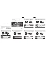
Gain and Offset
Analog Gain in the ADC
The only analog Gain available in the is located at the sensor level, in the ADC converter.
This “Preamp Gain” is in fact a variation of the ramp of the comparator of the ADC.
Then 3 Values are available : x1, x2 and x4. A gain x1 in a 12 bits conversion is equivalent to x4 in 10 bits.
x1
x2
x4
LSB
FWC
Comparator Ramps
at different Gains
or Format
Clamp (Black Ref)
Setting
1024
(10bits conversion)
electrons
4096
(12bits conversion)
x1
x2
x4
OUT
Pixel
X
Preamp
Gain
X
White Balance Gains
Red
Green
red
Green
blue
Blue
+
X
FFC
Offset Gain
X
FFC
Adjust
FPGA
Sensor
X
Quarter
(Tap)
Gains
Action on whole line
Action per pixel
Action per Sensor’s Quarter
Action per Color
(Not available on BA0 models)
X
Amp
Gain
X
X
X