CIRCUIT DESCRIPTION
3-6
February 2001
Part No. 001-9800-001
return-to-zero (NRZ) format consisting of one start bit,
eight or nine data bits, and one stop bit.
This port is used to provide data communication
with the computer used to program the transceiver.
Connection is made via the front panel microphone
connector. Another use for this port is data communi-
cation with an external data device such as a modem.
Connection is made via connector J301. Communica-
tion cannot occur simultaneously over both of these
paths.
Other General Purpose Inputs and Outputs
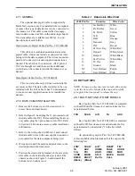
The PA0-PA7 pins are used for general purpose
inputs and outputs as follows:
PA0 -
Input for PTT signal from the microphone jack
and W302/W312 option slot wire-outs. This signal is
low when the transmitter is keyed.
PA1 -
Input for the receive LTR or Call Guard data
signal.
PA2 -
Service request input from microcontroller U2
on the display board. This tells U101 that it has data to
send on the SPI bus described previously.
PA3 -
Input from the Option 1 pin of modem
connector J301.
PA4/PA5 -
Transmit LTR/Call Guard data output.
These two outputs are used to create a pseudo sine-
wave signal. See Section 3.5.4 for more information.
PA6 -
Output for supervisory tones generated by the
microcontroller such as busy and out-of-range.
PA7 -
Input from the squelch circuit (see Section
3.4.4). When the received signal strength increases to
the squelch threshold level, this input goes high. The
microcontroller uses this information to determine
when receive data is valid and to control audio
muting.
3.3.2 MEMORY AND LATCH PROGRAMMING
RAM U107
When a data read or write to U107 occurs, the
location in U107 is selected by address lines A0-A12,
and the data appears on data bus lines D0-D7. Chip
select is performed by pulling the CE1 input (pin 20)
low. The CE2 input is always pulled high by R114.
The A13 and A14 address lines can be connected by
changing jumpers if a 16K or 32K part is required.
Data is read from U107 by pulling the OE input (pin
22) low. Likewise, data is written by pulling the WE
input (pin 27) low. See the U104 description which
follows for more information.
Flash EPROM (U108)
As described in Section 3.3.1, U108 can store up
to 128K bytes of data. The memory space is arranged
as 32K of common code space and twelve 8K blocks
of bank code space. The A15 line of the microcon-
troller determines if common or bank code space is
selected. When A15 is high, common space is
selected, and when it is low, bank space is selected.
The A15 line controls the four two-input multi-
plexers in U109. When A15 is low, the A input is
connected to Y which routes the PG0-PG3 outputs of
the microcontroller to U108. PG0-PG3 then select the
desired bank. Then when A15 is high, the B input is
routed to Y and the A13-A15 address lines of the
microcontroller are routed to U108.
Therefore, when a data read or write to U108
occurs, the lower 13 bits of the address are specified
by address lines A0-A12 and the rest of the address is
specified as just described. The data appears on data
bus lines D0-D7. Data is read from U108 by pulling
the OE input (pin 24) low, and data is written by
pulling the WE input (pin 31) low. Refer to the
following U104 description for more information.
Chip select is provided by pulling the CE input (pin
22) low.
Read/Write Strobe Select (U104A-D)
NAND gates U104C and U104B select the read
and write signals applied to U107 and U108. When a
memory read occurs, the R/W output of the microcon-
troller goes high. This signal is inverted by U104C and
applied to the OE of U108. When a memory write
operation occurs, the R/W output of the microcon-
troller goes low. U104B is then enabled by the high
output of U104C, and the high E signal is inverted by
U104B and applied to the WE pin of U107 and to
U104D.
AUDIO/LOGIC DESCRIPTION (ALL MODELS)


