background image

CIRCUIT DESCRIPTION

3-8

February 2001

Part No. 001-9800-001

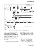
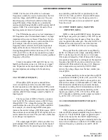
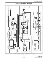
Figure 3-3   Audio and Data Processing Circuitry Block Diagram

Bandpass Filter/

De-Emphasis

300-3000 Hz

U301C,

U301D

U300B,

U300C

U304A

U303C

U304A

U300D,

U300A

U304B

Amplifier

Microphone

Amplifier

U301B

U303B

U307B

Q300

U305

U307C

Q301

Q307

Gain Adjust

U301A

Summing

Amplifier

Audio

Amplifier

U306

8V

Front Panel

Volume Control

(9842)

Q302

Low-Pass Filter

< 140/211 Hz

Filter Bandwidth Control

Data

Detector

Bandpass Filter

High Pass Filter

> 300 Hz

Low Pass Filter

< 140/211 Hz

Comparator

Digital

Squelch

Control

Microphone

U303D

Pre-Emphasis/

Limiter

Mic Audio

Gate

Tx

Data
Gate

U302B,

U302C

Amplifier

Splatter Filter

> 3 kHz

U303A

Rx Audio

Gate

Speaker

RECEIVE AUDIO

RECEIVE DATA

SQUELCH

TRANSMIT AUDIO

TRANSMIT DATA

Rx Audio/Data

From

Receiver

From
Logic

From
Logic

From
Logic

From
Logic

From
Logic

To Synthesizer

To Synthesizer

To Logic

From Logic

From Logic

To Logic

From
Logic

Serial Data

Mic Audio Gate Control

Tx Audio Gate Control

Data

Analog Transmit Data

Tx

Audio

Squelch Signal

Digital Receive Data

Audio Mute Control

Supervisory Tones

Rx Audio Gate Control

U308B

U309

Digital Volume

Control

(98x1)

Pin 5 is the input of an internal gain control stage. 

Gain increases in proportion to increases in the DC 
voltage on this pin. With the low tier models, volume 
control is provided by a D/A converter formed by shift 
register U309 and several resistors. The six-bit output 
controls the volume in 64 steps. U309 is programmed 
by the SPI bus described in Section 3.3.1. With the 
mid and high tier models, the front panel volume 
control is part of a voltage divider which includes 
R356 and R426. 

If the voltage on pin 5 falls below approximately 

0.4 volt DC, the output is muted. Speaker muting is 

controlled by the Q7 output (pin 12) of latch U110. 
When this output goes high, inverter/level translator 
Q302 turns on which grounds the volume control input 
of U306 and mutes the speaker.

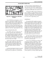
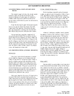
3.4.3 RECEIVE DATA PROCESSING

The receive audio/data signal from amplifier 

U301B is applied to a low-pass filter formed by 
U300B and U300C. This filter attenuates voice and 
harmonic frequencies occurring above the data band. 

AUDIO/LOGIC DESCRIPTION (ALL MODELS)

Summary of Contents for 001-9800-200

Page 1: ...ANUAL 984X SERIES UHF 988X SERIES 800 MHZ 989X SERIES 900 MHZ 25 or 40 Watts UHF 15 or 30 Watts 800 900 MHz 13 6 VDC Part No 242 98xx xxx First Printing January 2001 Supersedes Part No 001 9800 200 9...

Page 2: ...nd commercial customers The company designs manufactures and markets conventional and trunked radio systems mobile and portable subscriber radios repeaters and Project 25 digital radio products Viking...

Page 3: ...dels 2 9 3 CIRCUIT DESCRIPTION 3 1 GENERAL TRANSCEIVER DESCRIPTION 3 1 Introduction 3 1 Circuit Protection Fuses 3 1 Synthesizer 3 1 Audio Logic Board 3 1 Receiver 3 2 Transmitter 3 2 3 2 POWER DISTRI...

Page 4: ...ING 4 3 Introduction 4 3 Reference Oscillator U806 4 4 VCO Module 4 4 Synthesizer IC U804 4 4 Determining Synthesizer Counter Divide Numbers 4 5 4 4 RECEIVER SERVICING 4 5 4 5 TRANSMITTER SERVICING 4...

Page 5: ...wn 1 2 1 2 Identification Number Breakdown 1 3 1 3 98xx Accessories 1 3 2 1 Data Cable Wire Chart 2 8 4 1 Ceramic SMD Capacitor Identification 4 2 4 2 SMD Inductor Identification 4 3 LIST OF FIGURES 2...

Page 6: ...gh and low tier versions and the Multi Net LTR Net and SMARTNET SmartZone models are available in only the high tier version Therefore only high tier models are covered by this manual For servicing in...

Page 7: ...l is selected the deviation automatically changes to the level set in this screen 1 2 5 PROGRAMMING Transceiver programming is performed using a PC compatible computer the E F Johnson Remote Programmi...

Page 8: ...f Year Last Digit of Year A Waseca Type Plant From P N 1 Low pwr LTR 2 High pwr LTR 3 High pwr Data MN 4 Low pwr LTR Net 5 High pwr LTR Net 6 Low pwr Multi Net 7 High pwr Multi Net 8 Low pwr Data LTR...

Page 9: ...ndor kit includes a board assembly that installs in the option wire outs on the audio logic board to provide companding Likewise the encryption kit includes a board assembly that connects to the other...

Page 10: ...ortant as there are times when the technicians may have specific ques tions that need to be answered in order to completely identify and repair a problem When returning equipment for repair it is also...

Page 11: ...ts DC nominal negative ground Current Drain 300 mA maximum receive standby 1 5 A maximum receive rated audio output 10 0 A maximum transmit 25 W output 15 0 A maximum transmit 40 W output FCC Complian...

Page 12: ...equirement 13 6 volts DC nominal negative ground Current Drain 300 mA maximum receive standby 1 5 A maximum receive rated audio output 7 0 A maximum transmit 15 W output 11 0 A maximum transmit 30W ou...

Page 13: ...9 kg Power Requirement 13 6 volts DC nominal negative ground Current Drain 300 mA maximum receive standby 1 5 A maximum receive rated audio output 7 0 A maximum transmit 15 W output 11 0 A maximum tra...

Page 14: ...4 x 5 16 sheet metal 3 575 3604 010 11 5 4 7 ohm external spkr optional 250 0151 010 6 Hanger grounding wire assembly 023 7171 911 Miniature UHF Jack 1 2 2 3 4 5 6 7 8 11 10 Antenna 10 ft Install 15A...

Page 15: ...where it will be least likely to cause injury in case of an accident Airbags deploy with great force Therefore do not mount it anywhere near the deployment area In addition do not place any other obje...

Page 16: ...n control cable 11 ft opt 597 9800 009 8 Screw 4 24 x 5 16 sheet metal 3 575 3604 010 17 5 4 7 ohm external spkr optional 250 0151 010 NEG POS 1 2 3 Miniature UHF Jack Antenna 4 5 6 7 8 9 10 11 12 13...

Page 17: ...er cable wire to the negative battery terminal 5 Both 7 and 15 ampere fuses are included with the power cable Install the 15 ampere fuse in this application 6 Plug the power cable into the transceiver...

Page 18: ...are required and this section can be skipped However then be sure that the Ignition Sense Delay Time is set to Forever Infinite If it is not improper transceiver operation may result when starting the...

Page 19: ...level volume controlled speaker output It provides drive to an external device such as an audio power amplifier The input impedance of the external device should be greater than 20k ohms For this out...

Page 20: ...p to 5 watts of power a 4 7 ohm external speaker can be used This speaker is plugged into the external speaker jack on the back of the transceiver This is a standard 1 8 two conductor phone jack The i...

Page 21: ...4 for more accessory cable installation information 3 Refer to the wiring chart in Table 2 1 and connect the data cable wires to the user supplied connector as required for the data equipment being us...

Page 22: ...SMARTNET SmartZone transceiver This kit includes the five key caps listed below EMER F1 F2 F3 SCAN Key Cap Kit Part No 587 9840 105 is also included with each transceiver This kit includes the key cap...

Page 23: ...oard The other fuse F300 0 6A limits the current of the 8 volt supply fed to modem jack J301 For information on power distri bution and switching refer to Section 3 2 3 1 3 SYNTHESIZER The synthesizer...

Page 24: ...smitter if either are excessive 3 2 POWER DISTRIBUTION AND SWITCHING 3 2 1 POWER SWITCHING CONTROL A diagram of the power distribution and switching circuits is shown in Figure 3 1 The main power swit...

Page 25: ...ower Hold From Shift Reg U111 Q7 Unsw Bat Unsw Bat R170 From Ignition Switch This Resistor Installed If Ignition Sense Not Connected Q510 Supply Switching Circuit Interface Board High Tier Only Audio...

Page 26: ...M can be programmed many times does not require a constant power supply and retains data indefinitely Temporary data storage is provided by an internal 1K x 8 RAM in microcontroller U101 and by extern...

Page 27: ...and Option 2 slot wire out W311 PE7 This input senses the voltage on the IN3 pin of Option 1 slot wire out W301 Serial Peripheral Interface Port SPI OR Gate U103 This serial port is formed by the MOSI...

Page 28: ...CE2 input is always pulled high by R114 The A13 and A14 address lines can be connected by changing jumpers if a 16K or 32K part is required Data is read from U107 by pulling the OE input pin 22 low Li...

Page 29: ...e control signal comes from the Q0 output pin 19 of latch U111 Transistor Q305 inverts this signal and also provides level translation from 5 volt logic levels of U111 to the 8 volt logic levels of U3...

Page 30: ...nalog Transmit Data Tx Audio Squelch Signal Digital Receive Data Audio Mute Control Supervisory Tones Rx Audio Gate Control U308B U309 Digital Volume Control 98x1 Pin 5 is the input of an internal gai...

Page 31: ...e audio signal When no signal or a weak signal is being received there is a large amount of noise present Conversely when a strong signal is received there is very little noise present The receive aud...

Page 32: ...more information 3 5 4 TRANSMIT DATA CIRCUIT U302D U302A The transmit LTR data and Call Guard tone data signals are generated by the microcontroller on pins 37 and 38 The four logic combinations poss...

Page 33: ...U806 The fR input is 50 kHz for all UHF channels Therefore the reference divider in U804 divides the 14 850 MHz reference oscillator signal by 297 The TCXO frequency stability is 2 0 PPM so this is al...

Page 34: ...s adds capacitance to the tank circuit which lowers its reso nant frequency Capacitance is added to the circuit when the control signal is low Therefore the lowest frequency is selected when both cont...

Page 35: ...fer Amplifier Q506 Q507 Q508 Q509 Q600 Q601 Q504 Q505 First Amplifier Second Amplifier Third Amplifier Predriver 8V Transmit Switch Driver Final Antenna Switch Directional Coupler Harmonic Filter CR60...

Page 36: ...ce such as a modem without passing through the limiting and filtering circuitry The levels of the audio and data signals are set by digitally controlled variable resistors in U802 These resistors are...

Page 37: ...programmed N number is 83 in this example the divide number is always two higher 85 because of reset cycles and other effects Therefore the prescaler divides by 65 for 55 x 65 or 3575 input pulses It...

Page 38: ...ta line from the audio logic board J201 pin 14 is first shifted into U801 then U800 and then U802 Data is clocked through the devices by the CLOCK signal J201 pin 13 when the STROBE input J201 pin 12...

Page 39: ...mperature The output signal of Q201 is fed to another two pole bandpass filter similar to the one on the input of Q201 as described in the preceding section Imped ance matching with the filter is prov...

Page 40: ...IF signal is then applied to pin 18 amplified by an internal amplifier and then fed back out on pin 16 and applied to ceramic filter Z205 This filter is identical to Z206 and provides additional atten...

Page 41: ...d C530 The input level is set by R528 and R530 Biasing is provided by R520 and R525 and C525 C526 and C520 C521 decouple RF signals Impedance matching on the output is provided by L502 C570 C531 L506...

Page 42: ...control circuit monitors transmitter current by sensing the voltage drop across it 3 9 4 ANTENNA SWITCH The antenna switch circuit consists of Q602 CR601 CR603 several other components and also a sec...

Page 43: ...o cut back power when power amplifier temperature is excessive as just described U500A Q500 Q502 Operation The forward power signal from the directional coupler is applied to pin 2 of amplifier U500A...

Page 44: ...ivides the 14 850 MHz reference oscillator signal by 297 and with 800 MHz models it divides the 17 500 MHz reference oscillator signal by 350 The TCXO frequency stability is 1 5 PPM so this is also th...

Page 45: ...fer Amplifier Q506 Q507 Q508 Q509 Q600 Q601 Q504 Q505 First Amplifier Second Amplifier Third Amplifier Predriver 8V Transmit Switch Driver Final Antenna Switch Directional Coupler Harmonic Filter CR60...

Page 46: ...sed it presents a very high impedance Forward biasing of PIN diode CR901 adds capac itance to the tank circuit which lowers its resonant frequency The diode is forward biased in the normal mode and re...

Page 47: ...s multiplied CR800 decreases the time required to charge C814 when power is turned on If a noise pulse or other voltage change appears on the collector the base voltage does not change significantly b...

Page 48: ...frequency to be 5 or 8 times the channel spacing With 800 and 900 MHz channels modulo 8 is used to allow 6 25 kHz 12 5 kHz channel spacing The fV input is produced by dividing down the VCO frequency a...

Page 49: ...ed out of one device into another Programming is performed using the SPI serial port of the microcontroller described in Section 3 3 1 The input to the internal shift register of these devices is the...

Page 50: ...pole crystal filter With 800 MHz models it has a center frequency of 52 950 MHz and a 3 dB bandwidth of 15 kHz and with 900 MHz models it has a center frequency of 45 MHz and a 3 dB bandwidth of 7 5 k...

Page 51: ...pin 59 and used along with the squelch signal to determine receive signal strength R259 C304 and R258 C303 provide low pass filtering of the audio and RSSI signals and C305 and C306 decouple RF 3 12...

Page 52: ...tter in the transmit mode Switching transistor Q602 is controlled by the transmit signal from the Q7 output pin 11 of shift register U801 This is the same signal that controls transmit 8 volt supply s...

Page 53: ...r voltage is excessive as just described in Section 3 12 4 U500A Q500 Q502 Operation U500A is a differential amplifier which ampli fies the difference between the reference voltage on pin 3 and the fo...

Page 54: ...es the output voltage on pin 7 to increase The gain of each U500B input is set at about ten by R509 R504 and R502 R507 Emitter biasing for Q501 is provided by R506 and R511 Normally the output voltage...

Page 55: ...chanical parts 4 1 4 CONFIGURING TRANSCEIVER FOR TESTING Multi Net versions of this transceiver have a test mode which can be selected to perform testing This mode is described in Section 3 13 of the...

Page 56: ...lowed by a number to indicate the multiplier The values for both standards are shown in the following table For example if there is a single black E on the capacitor it uses the American standard and...

Page 57: ...ansistors and diodes are iden tified by a special number Refer to page 6 1 for more information 4 3 SYNTHESIZER TROUBLESHOOTING 4 3 1 INTRODUCTION When there is a synthesizer malfunction the VCO is us...

Page 58: ...ked on frequency it should be near the lower 1 1 V or upper 5 2 V end of its range Frequency Shift Inputs The pin shift signals on pins 4 and 3 should be as follows L 0V H 5V Frequency If the VCO is l...

Page 59: ...as follows L 0V H 5V 4 5 TRANSMITTER SERVICING To isolate a transmitter problem to a specific stage check the DC and RF voltages shown on the schematic diagram 4 6 AUDIO LOGIC BOARD SERVICING 4 6 1 D...

Page 60: ...HW006 Insert 2 56 RF brd 537 2501 031 HW007 Lockwasher No 2 596 2102 006 HW008 Washer split lock No 4 596 1304 008 HW009 Screw 6 32 x 1875 rd hd Torx 575 9406 406 HW 010 Screw 4 40 x 1 8 pan hd zps s...

Page 61: ...Ref No Description Part No Q 007 NPN general purpose 576 0003 658 Q 100 NPN UHF low noise 576 0003 651 R 001 Pot 50k ohm w push on sw 562 0018 075 R 002 22 ohm 10 2W wire wound 569 2004 220 R 003 47k...

Page 62: ...MHz 5 1 pF NPO 5 50V cer smd 510 3615 519 470 512 MHz C 205 47 pF NPO 5 50V cer smd 510 3601 470 430 470 MHz Ref No Description Part No 39 pF 5 NPO 50V cer smd 510 3615 390 470 512 MHz C 206 2 7 pF 5...

Page 63: ...50V cer smd 510 3601 689 430 470 MHz 5 6 pF 5 NPO 50V cer smd 510 3615 569 470 512 MHz Ref No Description Part No C 236 22 pF 5 NPO 50V cer smd 510 3615 220 430 470 MHz 18 pF 5 NPO 50V cer smd 510 361...

Page 64: ...d 510 3605 103 C 294 47 F 10V tantalum smd 510 2624 470 C 295 1 F X7R 10 50V cer smd 510 3606 104 C 296 01 F X7R 10 50V cer smd 510 3605 103 C 297 01 F X7R 10 50V cer smd 510 3605 103 C 298 01 F X7R 1...

Page 65: ...er smd 510 3601 101 all others C 529 12 pF NPO 5 cer smd 510 3601 120 unrevised 430 470 MHz 01 F X7R 10 50V cer smd 510 3605 103 all others Ref No Description Part No C 530 39 pF NPO 5 50V cer smd 510...

Page 66: ...20 revised 430 470 MHz 10 pF 5 NPO 50V cer smd 510 3615 100 470 512 MHz Ref No Description Part No C 548 10 F 25V tantalum smd 510 2627 100 unrevised 430 470 MHz 5 1 pF 5 NPO 50V cer smd 510 3615 519...

Page 67: ...510 4064 471 all others C 566 01 F X7R 10 50V cer smd 510 3605 103 unrevised 430 470 MHz Ref No Description Part No 100 pF NPO 5 50V cer smd 510 3601 101 all others C 567 33 pF 5 NPO 50V cer smd 510 3...

Page 68: ...0V cer smd 510 3615 240 430 470 MHz 40 watt 47 pF 5 NPO 50V cer smd 510 3615 470 470 512 MHz 25 watt 24 pF 5 NPO 50V cer smd 510 3615 240 470 512 MHz 40 watt C 617 47 pF 250V mini mica 510 0019 470 Re...

Page 69: ...cer smd 510 3615 120 430 470 MHz 40 watt 6 8 pF 5 NPO 50V cer smd 510 3615 689 470 512 MHz 40 watt C 645 47 pF 250V mini mica 510 0019 470 430 470 MHz 40 watt 39 pF 250V mini mica 510 0019 390 470 512...

Page 70: ...470 MHz 8 2 pF 5 NPO 50V cer smd 510 3615 829 all others CR 200 Pin switching diode 523 1504 001 CR 201 Band switching diode 523 1504 035 CR 202 Band switching diode 523 1504 035 Ref No Description P...

Page 71: ...air core inductor 542 0030 005 unrevised 430 470 MHz 6T 17 5 nH smd air core inductor 542 0030 006 all others Ref No Description Part No L 501 5T 18 5 nH smd air core inductor 542 0030 005 unrevised...

Page 72: ...03 658 Q 503 NPN general purpose 576 0003 658 unrevised 430 470 MHz PNP general purpose 576 0003 612 all others Q 504 PNP general purpose 576 0003 612 unrevised 430 470 MHz Ref No Description Part No...

Page 73: ...smd 569 0105 822 R 229 Zero ohm 5 1 8W smd 569 0105 001 R 231 4 7k ohm 5 1 8W smd 569 0105 472 R 232 4 7k ohm 5 1 8W smd 569 0105 472 Ref No Description Part No R 233 22k ohm 5 1 8W smd 569 0105 223 R...

Page 74: ...ers R 520 47 ohm 5 1 8W smd 569 0105 470 unrevised 430 470 MHz 47k ohm 5 1 8W smd 569 0105 473 all others Ref No Description Part No R 521 47 ohm 5 1 8W smd 569 0105 470 unrevised 430 470 MHz 4 7k ohm...

Page 75: ...470 MHz Ref No Description Part No 1 0k ohm 5 1 8W smd 569 0105 102 all others R 544 10 ohm 5 1 8W smd 569 0115 100 R 545 17 8k ohm 1 1 8W smd 569 0111 425 R 546 100 ohm 5 1 8W smd 569 0105 101 unrevi...

Page 76: ...escription Part No R 822 10k ohm 5 1 8W smd 569 0105 103 R 823 33k ohm 5 1 8W smd 569 0105 333 R 824 Zero ohm 5 1 8W smd 569 0105 001 R 825 100 ohm 5 1 8W smd 569 0105 101 R 826 10k ohm 5 1 8W smd 569...

Page 77: ...ef No Description Part No C 244 01 F X7R 10 50V cer smd 510 3605 103 C 245 100 pF 5 NPO 50V cer smd 510 3615 101 C 246 30 pF 5 NPO 50V cer smd 800 MHz models 510 3615 300 16 pF NPO 5 50V cer smd 900 M...

Page 78: ...smd 510 3615 439 C 523 10 pF NPO 5 50V cer smd 510 3601 100 Ref No Description Part No C 524 39 pF NPO 5 50V cer smd 510 3601 390 C 525 39 pF NPO 5 50V cer smd 510 3601 390 C 526 01 F X7R 10 50V cer...

Page 79: ...510 3601 331 Ref No Description Part No 150 pF NPO 5 50V cer smd 900 MHz models 510 3601 151 C 811 01 F X7R 10 50V cer smd 510 3605 103 C 812 100 pF NPO 5 50V cer smd 510 3601 101 C 813 01 F X7R 10 50...

Page 80: ...0 Fuse 4A smd very fast blow 534 5000 140 J 201 Connector 2 x 10 pin male RF bd 515 7100 944 J 501 Connector 1 x 8 pin male RF bd 515 7100 942 Ref No Description Part No J 600 Connector 8 pin female P...

Page 81: ...smd 569 0105 472 R 209 220 ohm 5 1 8W smd 569 0105 221 R 210 18 ohm 5 1 8W smd 569 0105 180 R 211 270 ohm 5 1 8W smd 569 0105 271 Ref No Description Part No R 212 270 ohm 5 1 8W smd 569 0105 271 R 213...

Page 82: ...3 R 526 100 ohm 5 1 8W smd 569 0115 101 Ref No Description Part No R 527 10 ohm 5 1 8W smd 569 0115 100 R 528 100 ohm 5 1 8W smd 569 0115 101 R 529 680 ohm 5 1 8W smd 569 0115 681 R 530 10 ohm 5 1 8W...

Page 83: ...ohm 5 1 8W smd 569 0105 181 R 833 15k ohm 5 1 8W smd 569 0105 153 R 834 12k ohm 5 1 8W smd 569 0105 123 Ref No Description Part No R 835 560 ohm 5 1 8W smd 569 0115 561 R 836 33k ohm 5 1 8W smd 569 0...

Page 84: ...md 510 3605 103 C 111 10 F 16V tantalum smd 510 2625 100 C 112 10 F 16V tantalum smd 510 2625 100 C 113 1 F X7R 10 50V cer smd 510 3606 104 C 114 1 F X7R 10 50V cer smd 510 3606 104 C 115 1 F X7R 10 5...

Page 85: ...CR 102 5 6V zener SOT 23 523 2016 569 CR 103 5 6V zener SOT 23 523 2016 569 CR 104 5 6V zener SOT 23 523 2016 569 CR 105 5 6V zener SOT 23 523 2016 569 CR 106 Switching diode SOT 23 523 1504 002 CR 1...

Page 86: ...3 R 118 470 ohm 5 1 8W smd 569 0105 471 R 119 47k ohm 5 1 8W smd 569 0105 473 Ref No Description Part No R 120 4 7k ohm 5 1 8W smd 569 0105 472 R 121 10k ohm 5 1 8W smd 569 0105 103 R 122 10k ohm 5 1...

Page 87: ...334 R 320 62k ohm 5 1 8W smd 569 0105 623 Ref No Description Part No R 321 470 ohm 5 1 8W smd 569 0105 471 R 322 10k ohm 5 1 8W smd 569 0105 103 R 323 62k ohm 5 1 8W smd 569 0105 623 R 324 33k ohm 5...

Page 88: ...69 0105 103 R 410 6 8k ohm 5 1 8W smd 569 0105 682 R 411 22k ohm 5 1 8W smd 569 0105 223 R 412 1 0k ohm 5 1 8W smd 569 0105 102 Ref No Description Part No R 413 1 0k ohm 5 1 8W smd 569 0105 102 R 414...

Page 89: ...PART NO 250 0740 300 C 001 3 3 F 16V tantalum chip 510 2625 339 C 002 220 pF 5 NPO 50V cer chip 510 3602 221 EP001 Contact 038 diameter 586 9008 100 EP002 Mic cord w mod connector 597 2002 113 EP004...

Page 90: ...PARTS LIST 5 31 February 2001 Part No 001 9800 001 FRONT PANEL EXPLODED VIEW MP700 MP701 HW703 3 HW701 2 Display Board A400 MP705 MP704 MP702 5 HW701 2 HW702 2 MP703 2 Interface Board A475...

Page 91: ...030 Mtg Kit MP1 HW009 2 MP010 HW009 2 MP016 MP015 HW003 7 RF Board MP003 MP012 HW001 4 Part of 030 Mtg Kit MP008 HW003 7 MP007 HW002 2 HW007 2 Power Amplifier Board Audio Logic Board HW003 5 MP013 MP...

Page 92: ...4 MP004 Part of 040 Mtg Kit MP001 Part of 040 Mtg Kit HW001 Part of 040 Mtg Kit HW002 Part of 040 Mtg Kit MP001 Display Cover HW009 2 MP001 Chassis HW009 2 MP011 HW009 2 MP010 W003 MP700 HW004 2 HW00...

Page 93: ...76 0004 098 4 576 0004 401 6 576 0004 402 7 576 0004 817 8 576 0006 027 9 576 0006 114 10 576 0006 120 11 576 0006 234 12 MO 576 0006 450 11 576 0007 013 2 Number on Schematic DIODES 523 1504 001 4D 5...

Page 94: ...6 2 February 2001 Part No 001 9800 001 AMPLIFIED DYNAMIC MICROPHONE SCHEMATIC AND MECHANICAL PARTS Part No 250 0740 300...

Page 95: ...6 3 February 2001 Part No 001 9800 001 TRANSCEIVER TOP PHOTO 800 MHZ SHOWN TRANSCEIVER BOTTOM PHOTO 800 MHZ 30W SHOWN RF Board PA Board Audio Logic Board...

Page 96: ...GND RESET SW BAT SERV RQST HANGER PBNO A PBNO B CW CCW J1 J2 J2 J1 8 12 9 10 8 7 11 2 3 4 5 1 DISPLAY HARNESS PART NO 023 9800 047 SOURCE SW BAT 5V R21 10k R18 10k R6 47k R7 47k 25 2 3 PA7 PC5 PD7 IRQ...

Page 97: ...R21 R18 12 1 R4 R41 R20 R26 R25 Q3 Q2 C3 14 U2 C1 R44 R27 C4 U1 81 51 DS1 DS2 DS4 100 1 31 U3 15 28 R45 C6 Q7 E B R43 R42 Q6 E B C R24 R23 DS3 R46 C J1 1 C C8 C2 R35 R39 R40 R30 R29 R14 R15 R49 R50 R3...

Page 98: ...7 IS 5 3 CI TC DC GND C9 001 CURRENT LIMITER CR8 Q1 3658 C6 1 R24 22k R2 22k SOURCE VCC 2 3 1 OUT GND IN C10 10 C4 1 C18 10 C11 10 C5 1 R7 3 01k C8 47 R8 47 5k CR5 R26 1 R16 22k J1 MIC AUDIO IN J8 RX...

Page 99: ...307 B5 C 500 B2 C 501 A2 B2 C 502 B2 C 503 A2 C 504 A2 C 505 A2 C 506 A3 C 507 A4 C 508 A4 C 509 A3 C 510 A4 C 511 A3 B2 C 512 A1 A4 C 513 A2 A3 C 514 B1 B2 C 515 A1 B2 C 516 A1 C1 C 517 B1 B2 C 518 B...

Page 100: ...CR507 A2 CR800 C1 CR801 C1 CR802 B2 EP001 A2 EP002 B1 EP003 B1 EP500 B1 EP501 A1 F 500 A3 J 201 A3 Comp Location J 501 A3 L 200 A4 L 201 B4 L 202 A5 L 203 A5 L 204 A5 L 205 B5 L 206 B5 L 207 B5 L 208...

Page 101: ...6 A2 C1 R 537 A2 A1 R 538 A2 A3 R 539 B3 R 540 B3 A2 R 541 A2 R 542 A2 R 543 B3 A2 R 544 B2 R 545 A2 R 546 C1 B3 R 547 B3 R 548 A2 R 549 A2 R 550 A2 B3 R 551 A2 Comp Location R 552 A2 R 553 A2 R 554 B...

Page 102: ...A4 C 301 A4 C 302 A4 C 303 B4 C 304 B4 C 305 C3 C 306 C3 C 500 B2 C 501 C2 C 502 B2 C 503 C2 C 504 C2 C 505 C2 C 506 C3 C 507 C4 C 508 C4 C 509 C3 C 510 C4 C 511 C3 C 512 C2 C 513 C1 C 514 C1 C 515 A...

Page 103: ...B5 R 217 B5 R 218 B5 R 219 B5 R 221 B5 R 222 B5 R 225 B4 R 226 B4 R 228 A5 Comp Location R 229 A5 R 230 A5 R 231 A4 R 232 A4 R 233 A5 R 234 A5 R 237 A5 R 238 A5 R 239 A5 R 240 A5 R 241 A5 R 242 A5 R 2...

Page 104: ...the audio logic board layout on pages 6 22 Refer to the grid around the board to determine the approximate location of a component Comp Location C 100 A3 C 101 C1 C 102 C1 C 103 C1 C 104 A1 C 105 C1...

Page 105: ...R 113 A2 R 114 A1 R 115 C2 R 116 B2 R 117 B2 R 118 C2 R 119 B2 R 120 B2 Comp Location R 121 A2 R 122 C1 R 123 B4 R 124 C1 R 125 A1 R 126 A1 R 127 B2 R 128 B4 R 129 C1 R 130 B2 R 131 C1 R 132 B4 R 133...

Page 106: ...B4 R 395 A4 R 397 A3 R 398 C3 R 399 C3 R 400 B4 R 401 B3 R 402 B4 R 403 B4 R 404 B4 R 405 A4 R 406 B4 R 407 B4 R 408 B4 R 409 A4 Comp Location R 410 B4 R 411 B4 R 412 B4 R 413 A4 R 414 B3 R 415 B4 R...

Page 107: ...W102 W104 W105 W106 W107 W108 RF OUT RF OUT 8V BUFFER AMPLIFIER A900 VCO MODULE BUFFER AMPLIFIER VCO 20 19 C306 100 C304 01uF Rx Audio Out RSSI Out PART OF J201 11 8V 8V Out C567 100 10 Sw Bat Out C5...

Page 108: ...C511 EP2 C500 R512 R514 R549 R508 R505 R500 CR502 CR504 Q516 C502 R515 U500 B C E R506 C514 C515 R526 C516 R847 R856 R830 R853 Q507 C540 R523 R844 R521 R833 C826 L801 C822 R843 R842 R827 CR801 A900 V...

Page 109: ...1 C648 C619 C626 C618 C623 C624 C622 R604 Q602 E B C R606 C604 C602 CR603 C649 C655 470 512 MHz Only 470 512 MHz 430 470 MHz C646 C119 L102 C124 R112 R108 C108 R109 C113 R110 R107 C100 C101 R101 L100...

Page 110: ...C619 5 1 C628 3 9 C629 3 9 C630 2 2 L602 C644 12 C647 12 C641 33 C631 33 L608 R612 330 EP603 C633 47 C645 47 Q600 4402 C632 56 C642 56 C646 43 C627 27 C616 24 DIRECTIONAL COUPLER RX RF OUT EP L607 7T...

Page 111: ...600 C611 C653 J600 1 8 C646 CR600 P1 C630 C628 R603 C629 CR601 R602 EP602 L607 C616 C627 C601 C600 C603 C607 R611 C652 C651 C648 C619 C626 C618 C623 C624 C622 R604 Q602 E B C R606 C604 C602 CR603 C649...

Page 112: ...676 SECOND MIXER DETECTOR Z206 WIDEBAND NARROWBAND Z202 W111 W109 W101 W103 W102 W104 W105 W106 W107 W108 RF OUT RF OUT 8V BUFFER AMPLIFIER A900 VCO MODULE BUFFER AMPLIFIER VCO 20 19 C306 100 C304 01u...

Page 113: ...8 C815 R838 C821 C816 C819 R831 R829 C832 C830 R818 C842 L802 C823 C824 R835 C811 C812 R825 C828 C829 U502 C843 C834 U801 CR211 C548 C511 C305 C805 R820 R828 C806 C801 C555 C506 Q517 R557 R812 R813 R8...

Page 114: ...DEBAND NARROWBAND Z202 W111 W109 W101 W103 W102 W104 W105 W106 W107 W108 RF OUT RF OUT 8V BUFFER AMPLIFIER A900 VCO MODULE BUFFER AMPLIFIER VCO 20 19 C306 100 C304 01uF Rx Audio Out RSSI Out PART OF J...

Page 115: ...C511 EP2 C500 R512 R514 R549 R508 R505 R500 CR502 CR504 Q516 C502 R515 U500 B C E R506 C514 C515 R526 C516 R847 R856 R830 R853 Q507 C540 R523 R844 R521 R833 C826 L801 C822 R843 R842 R827 CR801 A900 V...

Page 116: ...7 R611 C652 C651 C648 C619 C626 C618 C623 C624 C622 R604 Q602 E B C R606 C604 C602 CR603 C649 C655 470 512 MHz Only 470 512 MHz 430 470 MHz C646 C119 L102 C124 R112 R108 C108 R109 C113 R110 R107 C100...

Page 117: ...100 C625 2 7 C620 2 7 L603 C622 3 3 C623 3 3 C624 3 3 L604 C618 4 3 C626 4 3 C619 4 3 C628 3 0 C629 3 0 C630 1 5 L602 C644 6 8 C641 33 C631 33 L608 R612 100 EP603 C633 43 C645 39 Q600 4402 C632 27 C64...

Page 118: ...600 C611 C653 J600 1 8 C646 CR600 P1 C630 C628 R603 C629 CR601 R602 EP602 L607 C616 C627 C601 C600 C603 C607 R611 C652 C651 C648 C619 C626 C618 C623 C624 C622 R604 Q602 E B C R606 C604 C602 CR603 C649...

Page 119: ...C305 100 R259 330 C302 01uF C281 01uF C280 01uF R233 22k R234 22k CR207 R237 20k CR209 R239 510 R238 20k C276 01uF C289 01uF C291 01uF R241 20k R240 510 CR210 CR208 R242 20k R906 12k R904 10 C908 3 L...

Page 120: ...O2 CR210 CR208 CR209 CR207 R240 R241 R234 R280 C281 R239 C271 R238 C289 C268 C267 C265 R212 C231 C246 C245 R217 C291 R233 R237 C270 C272 C269 C266 R210 C232 R211 C264 R213 L214 L215 L213 Z204B Z204A Q...

Page 121: ...9 CR207 R240 R241 R234 R280 C281 R239 C271 R238 C289 C268 C267 C265 R212 C231 C246 C245 R217 C291 R233 R237 C270 C272 C269 C266 R210 C232 R211 C264 R213 L214 L215 L213 Z204B Z204A Q202 C E E B Q203 E...

Page 122: ...613 C612 R600 CR601 Q600 C E B R601 W502 W505 L601 C601 C600 C602 CR600 A20 POWER JACK ANTENNA JACK C634 C640 R615 W501 C924 C911 L904 R912 W107 W102 W100 W108 W101 C921 R908 C916 L906 W103 W106 W104...

Page 123: ...Q651 4817 C619 1uF EP601 UNSW BAT EP600 W501 W500 FINAL AMP POWER AMP MODULE 5 W503 W502 C634 39 ANTENNA SWITCH Q602 3658 R613 100k C620 1 L603 0033uH J603 A20 Power Jack 001uF 0 3 Tx 13 6 Rx 0 8 Tx...

Page 124: ...606 C632 C628 C636 RT601 C629 8 1 J600 C630 C631 C638 C637 W500 5 4 3 2 1 U600 C609 C610 C611 C608 C607 C606 C615 EP600 C604 C605 C603 R613 R612 R600 CR601 Q600 C E B R601 W502 W505 L601 C600 C601 C60...

Page 125: ...50k R316 47k U307D MC14066 CR301 CR302 R317 27k R303 100k CR301 U300A MC3303 R304 10k R311 20k C309 4 7 U301D MC3303 C315 4 7 R354 0 C325 047 U307C MC14066 R355 100k U301A MC3303 R353 18k C320 680pF R...

Page 126: ...R301 R306 C308 R317 W332 U300 7 1 8 14 R316 R308 R334 R348 U301 7 1 8 14 C324 C319 W323 9 CR302 R322 C310 C342 C344 Q306 C B E C341 R372 C336 C331 R380 R367 R378 R370 R382 CR110 R154 F100 C333 R369 R...

Page 127: ...Part Number 001 9800 001CD 1 01 hph Printed in U S A...

Reviews: