background image

NOTE : 

The voltage for parts in hot circuit is measured using
hot GND as a common terminal.

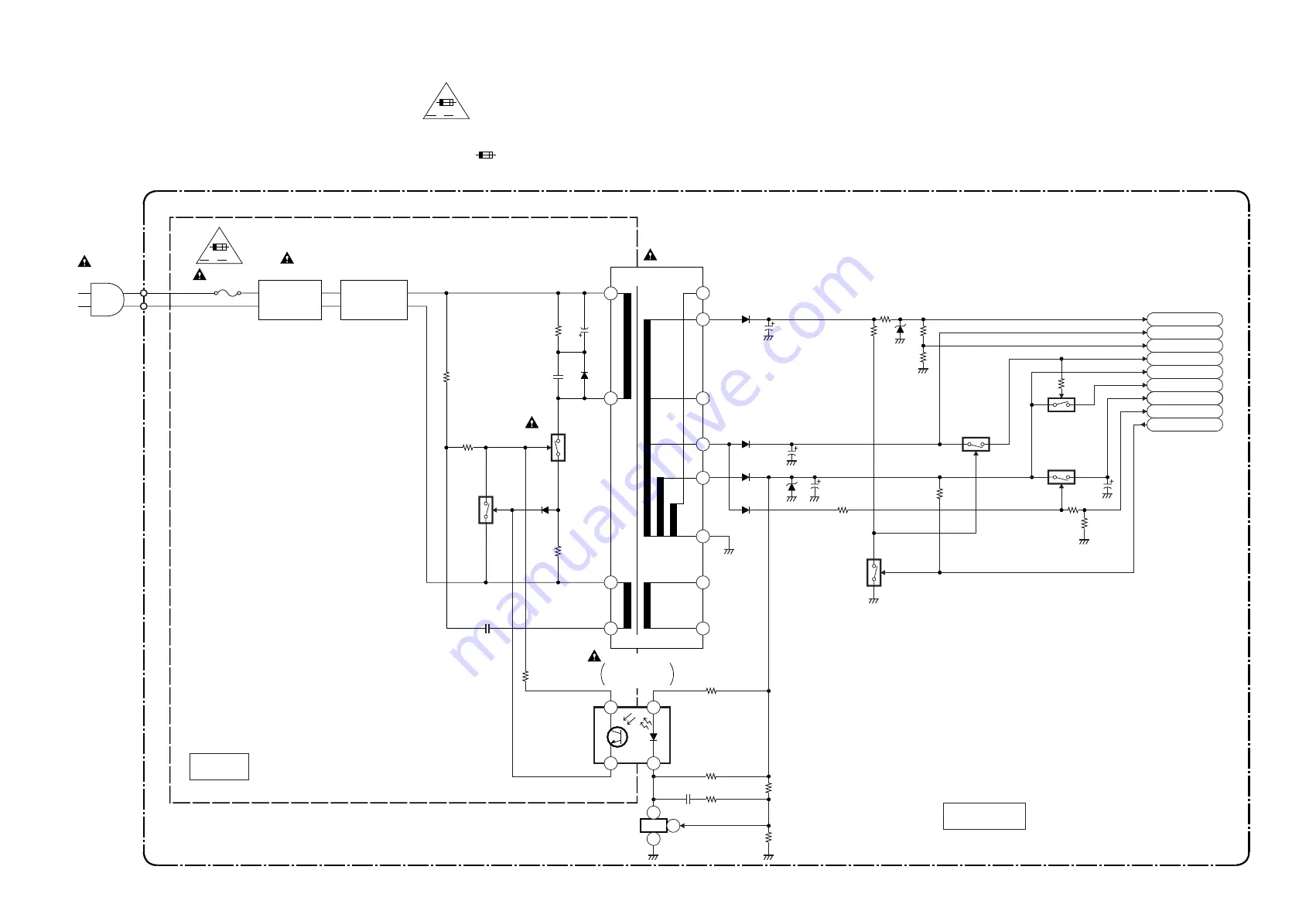
Power Supply Block Diagram

    A     V

HD230BLP

1-8-9

1-8-10

AC001

F001
1A 250V

LINE

FILTER

L001

D001 - D004

BRIDGE

RECTIFIER

Q001

Q002 

3

4

IC001

IC002

ERROR
VOLTAGE DET

T001

AL+12V
AL+15V
P-ON+9V

P-ON+5V

P-ON-L

AL+5V

TIMER+5V

P-DOWN-L

AL+33V

Q055

Q057

Q052

Q056

MAIN CBA

(SHUNT REGULATOR)

F

COLD

HOT

2

4

7

6

11

12

18

14

13

15

16

17

HOT CIRCUIT. BE CAREFUL.

1

2

REG

1

2

3

-REPLACE FUSE AS MARKED.

"Ce symbole reprèsente un fusible à fusion rapide."

CAUTION

FOR CONTINUED PROTECTION AGAINST FIRE HAZARD,
REPLACE ONLY WITH THE SAME TYPE FUSE.
ATTENTION : POUR UNE PROTECTION CONTINUE LES RISQES
D'INCELE N'UTILISER QUE DES FUSIBLE DE MÊME TYPE.

RISK OF FIRE

"This symbol means fast operating fuse."

    A     V

F

CAUTION !

Fixed voltage ( or Auto voltage selectable ) power supply circuit is used in this unit.
If Main Fuse (F001) is blown, check to see that all components in the power supply 
circuit are not defective before you connect the AC plug to the AC power supply. 
Otherwise it may cause some components in the power supply circuit to fail.

Summary of Contents for DCV203

Page 1: ...d Maintenance I Alignment for Mechanism I Disassembly Assembly of Mechanism I Alignment Procedures of Mechanism Sec 3 Exploded views and Parts List Section I Exploded views I Parts List DCV203 DCV603 CHANNEL POWER TAPE IN TIMER REC MENU VCR TV POWER VIDEO AUDIO REC OTR REW F FWD STOP EJECT PLAY MENU CHANNEL POWER REC OTR STOP EJECT REW PLAY F FWD TAPE IN VIDEO L AUDIO R TIMER REC VCR TV POWER ...

Page 2: ...injury to service personnel The possibility exists that improper ser vice methods may damage the equipment It also is important to understand that these CAUTIONS and NOTICES ARE NOT EXHAUSTIVE Funai could not possibly know evaluate and advice the service trade of all conceivable ways in which service might be done or of the possible hazardous consequences of each way Consequently Funai has not und...

Page 3: ...ructions 1 6 1 Electrical Adjustment Instructions 1 7 1 Block Diagrams 1 8 1 Function Indicator Symbols 1 8 11 Power Supply Trouble Shooting Guide 1 8 12 Schematic Diagrams CBA s and Test Points 1 9 1 Waveforms 1 10 1 Wiring Diagrams 1 11 1 System Control Timing Charts 1 12 1 IC Pin Function Descriptions 1 13 1 Lead Identifications 1 14 1 Sec 1 Main Section I Specifications I Preparation for Servi...

Page 4: ...st 1 4 Video Color S N AM R P dB 37 41 SP Mode 1 5 Video Color S N PM R P dB 30 36 SP Mode 1 6 Resolution PB Line 230 245 SP Mode 2 Servo 2 1 Jitter Low µsec 0 07 0 12 SP Mode 2 2 Wow Flutter 0 3 0 5 SP Mode 3 Normal Audio 3 1 Output PB dBV 9 6 3 SP Mode 3 2 Output R P dBV 9 6 1 5 SP Mode 3 3 S N R P dB 36 41 SP Mode 3 4 Distortion R P 1 0 4 0 SP Mode 3 5 Freq resp R P at 200Hz dB 11 4 SP Mode 20d...

Page 5: ...especially 1 Wires covered with PVC tubing 2 Double insulated wires 3 High voltage leads D Use specified insulating materials for hazardous live parts Note especially 1 Insulation tape 2 PVC tubing 3 Spacers 4 Insulators for transistors E When replacing AC primary side components transformers power cord etc wrap ends of wires securely about the terminals before solder ing F Observe that the wires ...

Page 6: ... and externally exposed accessible parts RF termi nals antenna terminals video and audio input and output terminals microphone jacks earphone jacks etc is lower than or equal to the specified value in the table below Measuring Method Power ON Insert load Z between B earth ground power cord plug prongs and exposed accessible parts Use an AC voltmeter to measure across the terminals of load Z See Fi...

Page 7: ...e the flat pack IC with tweezers while apply ing the hot air 3 Bottom of the flat pack IC is fixed with glue to the CBA when removing entire flat pack IC first apply soldering iron to center of the flat pack IC and heat up Then remove glue will be melted Fig S 1 6 4 Release the flat pack IC from the CBA using twee zers Fig S 1 6 Caution 1 Do not supply hot air to the chip parts around the flat pac...

Page 8: ... pins of the flat pack IC you can remove it easily Fig S 1 3 2 Affix the wire to a workbench or solid mounting point as shown in Fig S 1 5 3 While heating the pins using a fine tip soldering iron or hot air blower pull up the wire as the solder melts so as to lift the IC leads from the CBA contact pads as shown in Fig S 1 5 4 Bottom of the flat pack IC is fixed with glue to the CBA when removing e...

Page 9: ...ur due to a potential difference caused by electro static charge during unpacking or repair work 1 Ground for Human Body Be sure to wear a grounding band 1MΩ that is prop erly grounded to remove any static electricity that may be charged on the body 2 Ground for Workbench Be sure to place a conductive sheet or copper plate with proper grounding 1MΩ on the workbench or other surface where the semi ...

Page 10: ...to the Deck Mechanism Assembly and press the PLAY button The tape will be loaded into the Deck Mechanism Assembly Make sure the power is on TP502 SENSOR INHIBITION to GND This will stop the function of Tape Start Sensor Tape End Sen sor and Reel Sensors If these TPs are connected before plugging in the unit the function of the sensors will stay valid See Fig 1 Note Because the Tape End Sensors are...

Page 11: ... 22 Install two AA batteries supplied matching the polarity indicated on the bottom of the remote control 1 Cassette Compartment 2 F FWD button 3 PLAY button 4 REW button 5 STOP EJECT button 6 REC OTR button 7 MENU button 18 Display Window 19 Remote Sensor 10 CHANNEL buttons 11 POWER button 12 AUDIO Input jack 13 VIDEO Input jack 14 POWER indicator 15 VCR TV indicator 16 TAPE IN indicator 17 TIMER...

Page 12: ... 20 21 24 23 22 Install two AA batteries supplied matching the polarity indicated on the bottom of the remote control 1 Cassette Compartment 2 F FWD button 3 PLAY button 4 REW button 5 STOP EJECT button 6 REC OTR button 7 MENU button 18 Indicators 19 Remote Sensor 10 CHANNEL buttons 11 POWER button 12 AUDIO Input jacks 13 VIDEO Input jack 14 POWER indicator 15 VCR TV indicator 16 TAPE IN indicator...

Page 13: ...Reference Notes Reference Notes CAUTION Locking Tabs L 1 and L 2 are fragile Be careful not to break them 1 Remove five Screws S 2 Then slowly lift the VCR Chassis Unit Deck Assembly and Main CBA up 2 When reassembling solder wire jumpers as shown in Fig D4 3 Before installing the Deck Assembly be sure to place the pin of LD SW on Main CBA as shown in Fig D5 Then install the Deck Assembly while al...

Page 14: ...4 Deck Assembly FE Head Cylinder Assembly AC Head Assembly 5 Main CBA BOTTOM VIEW From FE Head From Cylinder Assembly From AC Head Assembly Lead with blue stripe Printing side Lead with blue stripe From Capstan Motor Assembly Lead connections of Deck Assembly and Main CBA Desolder Desolder Fig D4 ...

Page 15: ...1 6 3 HD300DC LD SW Pin Hole Hole Shaft Cam Gear 5 Main CBA 4 Deck Assembly 5 Main CBA SW507 LD SW Pin Fig D5 ...

Page 16: ...illoscope Dual trace with 10 1 probe V Range 0 001 50V Div F Range DC AC 20MHz 2 Alignment Tape FL8A Head Switching Position Adjust ment Purpose To determine the Head Switching point during playback Symptom of Misadjustment May cause Head Switching noise or vertical jitter in the picture Reference Notes Playback the Alignment tape and adjust VR501 so that the V sync front edge of the CH1 video out...

Page 17: ...L TRICK H SP LP SLP 26 SP LP SLP P ON L 22 P ON L P DOWN L 1 P DOWN L H A SW 79 H A SW H A COMP 80 H A COMP D PB L D REC H SW511 REC SW FROM TO VIDEO BLOCK TO AUDIO BLOCK FROM TO Hi Fi AUDIO BLOCK 1 8 1 1 8 2 HD230LS WF6 WF7 CLOCK DATA TU701 TUNER UNIT 23 INSEL ST SL INSEL ST SL 16 11 12 VCR TV 5 VCR TV IND 72 TIMER IND 75 REC IND 70 REC IND 71 D562 VCR TV D563 TAPE IN D564 TIMER D565 REC D561 POW...

Page 18: ... IC301 VIDEO SIGNAL PROCESS HEAD AMP 35 REC VIDEO SIGNAL PB VIDEO SIGNAL MODE SP REC 13 88 89 90 91 42 40 CHARA MIX 6dB AMP ENV DET AGC AMP HPF FROM TO SERVO SYSTEM CONTROL BLOCK FROM TO SERVO SYSTEM CONTROL BLOCK CYLINDER ASSEMBLY R L RF SW RF SW 93 V ENV H A SW H A COMP H A COMP TP302 WF2 VIDEO L 2 HEAD VIDEO R 2 HEAD TP301 C PB BUFFER D V SYNC C SYNC SP LP SLP SP LP SLP C ROTA D V SYNC C ROTA 3...

Page 19: ...UDIO HEAD AUDIO ERASE HEAD AC HEAD ASSEMBLY FE HEAD DECK ASSEMBLY 1 AE H FE H 2 FE H GND CL501 1 8 5 1 8 6 HD230BLA MAIN CBA PB AUDIO SIGNAL REC AUDIO SIGNAL Mode SP REC 16 11 12 D REC H D REC H REC EE PB A MUTE H D PB L FROM SERVO SYSTEM CONTROL BLOCK FULL ERASE HEAD WF4 78 80 2 SIF A IN L A IN R A IN L F A IN R F A OUT R N A OUT MOD A N A IN JK751 JK752 JK754 JK755 A OUT R A OUT L A IN L A IN R ...

Page 20: ...80 2 78 37 38 54 77 1 39 26 24 27 SIF A IN R A IN L N A OUT A IN R F A IN L F LIM 49 MUTE A OUT L MOD A A OUT R N A IN Hi Fi H SW A MUTE H NORMAL H 40 ST SAP MODE TO AUDIO BLOCK IIC BUS SDA IIC BUS SCL P ON 9V TO SERVO SYSTEM CONTROL BLOCK Hi Fi AUDIO R HEAD Hi Fi AUDIO L HEAD CYLINDER ASSEMBLY MAIN CBA Hi Fi A R 7 Hi Fi COM 8 Hi Fi A L 9 CL253 IC451 MTS SAP Hi Fi AUDIO PROCESS Hi Fi HEAD AMP Hi F...

Page 21: ... 3 REPLACE FUSE AS MARKED Ce symbole reprèsente un fusible à fusion rapide CAUTION FOR CONTINUED PROTECTION AGAINST FIRE HAZARD REPLACE ONLY WITH THE SAME TYPE FUSE ATTENTION POUR UNE PROTECTION CONTINUE LES RISQES D INCELE N UTILISER QUE DES FUSIBLE DE MÊME TYPE RISK OF FIRE This symbol means fast operating fuse A V F CAUTION Fixed voltage or Auto voltage selectable power supply circuit is used i...

Page 22: ...l and capstan mechanism is not functioning correctly 2 When tape loading mechanism is not functioning correctly 3 When cassette loading mechanism is not functioning correctly 4 When the drum is not working properly Cassette in H Cassette out L Cassette in Cassette in Cassette in Cassette in Blinks at 0 8Hz interval Blinks at 1 6Hz interval Blinks at 3 2Hz interval Blinks at 6 4Hz interval TIMER Ti...

Page 23: ...ating Per form check according to the step 1 and 2 of repair method 1 and check the following parts Remove the part from PCB Switching FET Q001 source resistor R014 gate resistor R008 and start resistor R004 and R005 Repair method 3 A circuit to turn on switching FET Q001 may not work and this may be regarded as a cause of trouble Even if the load at the secondary side is short circuited it cannot...

Page 24: ...dentified by the mark in the schematic diagram and the parts list Before replacing any of these components read the parts list in this manual carefully The use of substitute replacement parts that do not have the same safety characteristics as speci fied in the parts list may create shock fire or other hazards Capacitor Temperature Markings Capacitors and transistors are represented by the fol low...

Page 25: ...bility of repaired units use only original replacement parts which are listed with their part numbers in the parts list section of the service manual 4 Wire Connectors 1 Prefix symbol CN means connector can disconnect and reconnect 2 Prefix symbol CL means wire solder holes of the PCB wire is soldered directly 5 Mode SP REC 6 Voltage indications for PLAY and REC modes on the schematics are as show...

Page 26: ...l REC Video Signal Main 1 5 Schematic Diagram 1 9 3 1 9 4 HD230SCM1 MAIN 1 5 Schematic Diagram Parts Location Guide Ref No Position IC501 C 3 L501 A 1 L502 E 4 L503 E 3 L504 E 3 Q501 D 1 Q506 A 3 TP505 B 3 TP513 B 4 TEST POINTS TRANSISTORS ICS COILS ...

Page 27: ...C Video Signal Main 2 5 Schematic Diagram 1 9 5 1 9 6 HD230SCM2 MAIN 2 5 Schematic Diagram Parts Location Guide Ref No Position L701 I 1 Q503 K 4 Q504 K 4 Q562 H 3 Q563 I 3 TP502 H 4 TP506 K 4 TP751 K 2 TP753 K 2 TP754 K 2 TRANSISTORS TEST POINTS COILS ...

Page 28: ...matic Diagram 1 9 7 1 9 8 HD230SCM3 MAIN 3 5 Schematic Diagram Parts Location Guide Ref No Position IC301 N 2 L251 N 4 L303 N 4 L304 N 4 L421 N 1 L422 N 1 Q301 Q 3 Q302 Q 4 Q303 Q 4 Q391 Q 1 Q421 N 1 Q422 N 1 Q425 N 1 Q426 M 1 TP301 O 4 TP302 P 1 COILS ICS TRANSISTORS TEST POINTS ...

Page 29: ...ans fast operating fuse Ce symbole reprèsente un fusible à fusion rapide CAUTION Fixed voltage or Auto voltage selectable power supply circuit is used in this unit If Main Fuse F1001 is blown check to see that all components in the power supply circuit are not defective before you connect the AC plug to the AC power supply Otherwise it may cause some components in the power supply circuit to fail ...

Page 30: ...Video Signal REC Audio Signal REC Video Signal Main 5 5 Schematic Diagram DCV603 1 9 11 1 9 12 HD441SCM5 MAIN 5 5 Schematic Diagram Parts Location Guide Ref No Position IC451 X 2 L452 AA 4 TP452 AA 3 TEST POINTS COILS ICS ...

Page 31: ...ON FOR CONTINUED PROTECTION AGAINST FIRE HAZARD REPLACE ONLY WITH THE SAME TYPE FUSE ATTENTION POUR UNE PROTECTION CONTINUE LES RISQES D INCELE N UTILISER QUE DES FUSIBLE DE MÊME TYPE RISK OF FIRE REPLACE FUSE AS MARKED This symbol means fast operating fuse Ce symbole reprèsente un fusible à fusion rapide CAUTION Fixed voltage or Auto voltage selectable power supply circuit is used in this unit If...

Page 32: ... Fixed voltage or Auto voltage selectable power supply circuit is used in this unit If Main Fuse F1001 is blown check to see that all components in the power supply circuit are not defective before you connect the AC plug to the AC power supply Otherwise it may cause some components in the power supply circuit to fail MAIN CBA Parts Location Guide Ref No Position IC001 F 2 IC002 F 1 IC301 D 3 IC45...

Page 33: ...013 BHD400F01014 is used for the Main CBA in this S M NOTE The voltage for parts in hot circuit is measured using hot GND as a common terminal BECAUSE A HOT CHASSIS GROUND IS PRESENT IN THE POWER SUPPLY CIRCUIT AN ISOLATION TRANSFORMER MUST BE USED ALSO IN ORDER TO HAVE THE ABILITY TO INCREASE THE INPUT SLOWLY WHEN TROUBLESHOOTING THIS TYPE POWER SUPPLY CIRCUIT A VARIABLE ISOLATION TRANSFORMER IS ...

Page 34: ... Fixed voltage or Auto voltage selectable power supply circuit is used in this unit If Main Fuse F1001 is blown check to see that all components in the power supply circuit are not defective before you connect the AC plug to the AC power supply Otherwise it may cause some components in the power supply circuit to fail MAIN CBA Parts Location Guide Ref No Position IC001 F 2 IC002 F 1 IC301 D 3 IC45...

Page 35: ... 10 50usec PLL DATA 0 1V x 10 2msec C PB 10mV x 10 RF SW 0 5V x 10 5msec TU VIDEO 20mV x 10 10usec MOD V 20mV x 10 2msec PLL CLK 0 1V x 10 2msec WAVEFORMS 1 10 1 U27WFF TP751 of Main CBA TP751 of Main CBA TP302 of Main CBA UPPER LOWER TP302 of Main CBA Pin 2 of TU701 Pin 14 of TU701 Pin 12 of TU701 Pin 11 of TU701 Pin 6 of TU701 Pin 18 of TU701 TP301 of Main CBA ...

Page 36: ... REV 7 D CONT 8 D PFG 9 GND 10 AL 12V 11 AL 15V 12 AE H FE H 1 FE H GND 2 CL501 CL502 CL504 CL253 CAPSTAN MOTOR FULL ERASE HEAD FE HEAD VIDEO R 1 HEAD VIDEO L 1 HEAD AC CORD ANT IN ANT OUT VIDEO OUT AUDIO IN R AUDIO IN L VIDEO IN AUDIO OUT R AUDIO OUT L REAR VIDEO IN AUDIO IN R AUDIO IN L FRONT VIDEO L 2 HEAD VIDEO R 2 HEAD Hi Fi AUDIO R HEAD Hi Fi AUDIO L HEAD M DRUM MOTOR PG SENSOR MAIN CBA BHD4...

Page 37: ...EJ 4 51V 5 00V 5 00V CL 0 00V 0 25V 0 00V SB 1 06V 1 50V 1 21V TL 0 66V 1 05V 0 91V FB 1 99V 2 60V 2 17V SF 1 51V 1 98V 1 80V SM 3 20V 3 75V 3 40V AU 0 26V 0 65V 0 44V AL 4 51V 5 00V 5 00V SS 2 61V 3 19V 2 97V RS Symbol Loading Status EJ Eject CL Eject REW Reel SB REW Reel Stop B TL Stop B Brake Cancel FB Brake Cancel FF REW SF FF REW Stop M FF REW SM Stop M FF REW Stop A AU Stop A Play REC AL Pla...

Page 38: ... CL EJ SS SS AU AU TL LD SW CL SS LM FWD M REV C DRIVE Z ON ON C F R DRUM ROTATION P ON A MUTE H D REC H D PB L PAUSE ON PAUSE PAUSE ON PAUSE OFF PAUSE OFF AU AL AU SF SM EJ AU RS SF SM TL FB AL SB 74 21 27 22 7 23 24 TV VCR 77 POWER OFF STOP PLAY RS FS PLAY STILL STOP PLAY DISPLAY 0 1S SB TL SB FB SM SM SF AL AL RS AU AL SM 0 8S 0 2S 0 3S 1 0S 0 2S 1 5S 2H 2 5S 4H 1 0S 0 2S 0 8S 0 2S 1 2S 0 2S 20...

Page 39: ... STOP A LD REV FF LD REV LD REV LD FWD LD FWD LD FWD LD FWD LD FWD LD FWD LD FWD REC PAUSE REC REC REW LD REV LD REV LD REV LD REV LD REV LD REV LD REV PAUSE REC or PAUSE STOP EJECT STOP EJECT STOP EJECT 2 STOP A FF STOP A REW STOP A REC PAUSE PAUSE or REC STOP A EJECT STOP FF STOP REW STOP REC REC REC PAUSE STOP TL TL SM SM SF SF AL AL SM AL AL AL AU AU SM TL SB EJ RS RS SM SM SF FB SM AU AU SS S...

Page 40: ...9 H A SW 78 ROTA AT H Z H L L ST BL STILL FRAME ADVANCE STILL The first rise of RF SW after a rise in F AD signal Stop detection T2 Slow Tracking Value Acceleration Detection T1 Reversal Limit Value 20ms DCV603 Still Slow Control Frame Advance Timing Chart 1 SP Mode Fig 3 ...

Page 41: ...l Signal C DRIVE PB CTL 27 C F R 79 H A SW 78 ROTA STILL STILL AT ST BL Stop detection T2 Acceleration Detection T1 Slow Tracking Value Reversal Limit Value FRAME ADVANCE The first rise of RF SW after a rise in F AD signal 20ms 2 LP SLP Mode Fig 4 ...

Page 42: ...D REV LD REV 0 2S 0 5S PIN NO CL EJ SS SS AU AU TL LD SW CL SS LM FWD M REV C DRIVE Z ON ON C F R DRUM ROTATION P ON A MUTE H D REC H D PB PAUSE SLOW AU AL AL AU SF SM EJ AU RS SF SM TL FB AL SB 74 21 27 22 7 23 24 TV VCR 77 POWER OFF STOP PLAY RS FS STILL SLOW PLAY STOP PLAY DISPLAY 0 1S SB TL SB FB SM SM SF AL AL RS AU AL SS AU AL SM 0 8S 0 2S 0 3S 1 0S 0 2S 1 5S 2H 2 5S 4H 0 5S 0 2S 0 8S 2H 1 2...

Page 43: ... STOP A LD REV FF LD REV LD REV LD FWD LD FWD LD FWD LD FWD LD FWD LD FWD LD FWD REC PAUSE REC REC REW LD REV LD REV LD REV LD REV LD REV LD REV LD REV PAUSE REC or PAUSE STOP EJECT STOP EJECT STOP EJECT 2 STOP A FF STOP A REW STOP A REC PAUSE PAUSE or REC STOP A EJECT STOP FF STOP REW STOP REC REC REC PAUSE STOP TL TL SM SM SF SF AL AL SM AL AL AL AU AU SM TL SB EJ RS RS SM SM SF FB SM AU AU SS S...

Page 44: ... H L 13 OUT IIC BUS SCL IIC BUS Control Clock H L 14 N U Not Used 15 N U Not Used 16 OUT INSEL ST SL Input Selector Control Signal EE Rec Still Slow Playback H Hi z L 17 OUT PIC TURE SEL PictureControl Signal 18 OUT RF SW Video Head Switching Pulse H L 19 OUT D V SYNC Dummy V sync Output H Hi z 20 IN RESET System Reset Signal Reset L L 21 OUT LM FWD REV Loading Motor FWD REV Output H Z L 22 OUT P ...

Page 45: ... IN OUT Signal Name Function Active Level 56 IN OUT CTL Playback RecordControl Signal 57 IN OUT CTL Playback RecordControl Signal 58 OUT CTL Amp Output Control Signal for Test Point 59 A N U Not Used B IN HiFi NOR IN Audio Mode Input HiFi L Normal H A D 60 N U Not Used 61 A N U Not Used B IN ST SAP IN Tuner Stereo Sap Detector Signal Input A D 62 IN END S Tape End Position Detect Signal A D 63 IN ...

Page 46: ...R IND TIMER LED Signal Output L 76 OUT CONV SW RF Conv Out put Channel Switching Sig nal 3ch Hi z 4ch L Hi z L 77 OUT VCR TV RF Conv ON OFF Signal TV L VCR H H L 78 OUT C ROTA Color Phase Rotary Changeover SIgnal H L 79 OUT H A SW Video Head Amp Switching Pulse H L 80 IN H A COMP Head Amp Comparator Signal H L Pin No Mark IN OUT Signal Name Function Active Level ...

Page 47: ... GR TPE2 2SC2120 Y TPE2 KTC3203 Y 2SA1015 GR TPE2 KTC3198 Y GR E C B A K C E LTV 817 B C F EL817 A B K A R KIA431 AT KIA431A AT TL431A TA 81 80 31 100 50 30 1 51 LA71091M MID 32A22 PT204 6B 12 E C Note A Anode K Cathode E Emitter C Collector B Base R Reference G Gate D Drain S Source RN1511 TE85R FMG4A T148 B1 B2 C2 C1 E S D G 2SK3374 2SK3472 LEAD IDENTIFICATIONS ...

Page 48: ...ice Fixtures and Tools 2 2 1 Mechanical Alignment Procedures 2 3 1 Disassembly Assembly Procedures of Deck Mechanism 2 4 1 Alignment Procedures of Mechanism 2 4 9 Sec 2 Deck Mechanism Section I Standard Maintenance I Alignment for Mechanism I Disassembly Assembly of Mechanism I Alignment Procedures of Mechanism ...

Page 49: ...l only H Hours Check I Change Deck Periodic Service Schedule Ref No Part Name 1 000 H 2 000 H 3 000 H 4 000 H B2 Cylinder Assembly I I B3 Loading Motor Assembly I B8 Pulley Assembly I I B587 Tension Lever Assembly I I B31 AC Head Assembly I B573 B574 Reel SP D2 Reel TU D2 I B37 Capstan Motor I I B52 Cap Belt I I B73 FE Head I B133 B134 Idler Gear Idler Arm I I B410 Pinch Arm Assembly I I B414 M Br...

Page 50: ... hard material but since it is very thin avoid cleaning it vertically 2 Wait for the cleaned part to dry thoroughly before operating the unit 3 Do not reuse a stained head cleaning stick or a stained chamois cloth Cleaning of Audio Control Head Clean the head with a cotton swab Procedure 1 Remove the top cabinet 2 Dip the cotton swab in 90 isopropyl alcohol and clean the audio control head Be care...

Page 51: ...2 Alignment Tape FL8N 2Head only FL8NW 4Head only Azimuth and X Value Adjustment of Audio Control Head Adjustment of Envelope Waveform J 2 Guide Roller Adj Screwdriver Available Locally Guide Roller J 3 Mirror Available Locally Tape Transportation Check J 4 Azimuth Adj Screwdriver Available Locally A C Head Height J 5 X Value Adj Screwdriver Available Locally X Value ...

Page 52: ...that the Moving guide preparations are in the Eject Position 4 Turn the LDG Belt in the appropriate direction shown in Fig M1 until the Moving guide prepara tions come to the Eject Position Stop turning when the preparations begin clicking or can not be moved further However the tape will be left wound around the cylinder 5 Turn the LDG Belt in the appropriate direction con tinuously and the casse...

Page 53: ... the X value and envelope Not good Do the final tape traveling test to see that the tape runs normally in play mode with out creasing or slacking Completion Not good OK OK OK Not good Not good OK Flowchart of Alignment for tape traveling 1 A 1 A 1 B 1 C 1 C 1 D 1 D 1 B 1 C 1 B 1 C 1 A 1 Tape Interchangeability Alignment Note To do these alignment procedures make sure that the Tracking Control Circ...

Page 54: ...ition of the Audio Control Erase Head Symptom of Misalignment If the Horizontal Position of the Audio Control Erase Head is not properly aligned maximum envelope can not be obtained at the Neutral position of the Tracking Control Circuit 1 Connect the oscilloscope to TP301 C PB and TP513 CTL on the Main CBA Use TP302 RF SW as a trigger 2 Playback the Gray Scale of the Alignment Tape FL8NW and conf...

Page 55: ...of Guide Roller 2 Refer to Fig M3 so that the waveform looks like the one shown in Fig M9 4 If the envelope is as shown in Fig M8 adjust the height of Guide Roller 3 Refer to Fig M3 so that the waveform looks like the one shown in Fig M9 5 When Guide Rollers 2 and 3 Refer to Fig M3 are aligned properly there is no envelope drop either at the beginning or end of track as shown in Fig M9 Note Upon c...

Page 56: ...DM1 DM6 Desolder 3 S 2 8 8 Loading Motor Assembly T DM1 DM7 Desolder LDG Belt 2 S 3 9 9 AC Head Assembly T DM1 DM7 S 4 10 2 Tape Guide Arm Assembly T DM1 DM8 P 2 11 10 C Door Opener T DM1 DM8 L 4 12 11 Pinch Arm B T DM1 DM8 P 3 13 12 Pinch Arm Assembly T DM1 DM8 14 14 FE Head Assembly T DM1 DM9 S 5 15 15 Prism T DM1 DM9 S 6 16 2 15 Sensor Gear T DM1 DM15 17 2 Slider Shaft T DM10 L 5 18 17 C Drive ...

Page 57: ...or Installation Refer to Deck Exploded Views for lubrication 33 32 Loading Arm TU Assembly B DM2 DM14 Refer to Alignment Sec Pg 2 4 9 34 2 25 M Brake TU Assembly T DM1 DM15 P 7 Brake Belt 35 2 25 M Brake SP Assembly T DM1 DM15 P 8 36 35 Tension Lever Assembly T DM1 DM15 37 36 T Lever Holder T DM15 L 12 38 34 Reel TU D2 T DM1 DM15 39 38 M Gear T DM1 DM15 40 36 Reel SP D2 T DM1 DM15 41 32 36 Moving ...

Page 58: ...2 4 3 U27NDA 14 13 11 10 12 7 46 8 30 40 16 39 38 42 41 43 9 34 15 36 35 Fig DM1 Top View 29 32 20 33 24 25 27 26 23 28 31 21 22 Fig DM2 Bottom View ...

Page 59: ... pull up the right side on 2 to release Pin A and Pin B from the slots A Then remove Pin C and Pin D on 2 from the slots B as shown Fig DM4 2 Pin A Slots B Pin C Pin B Pin D Pull up Slide Slot A Slot A 1 2 A 3 4 5 6 L 1 L 2 P 1 Fig DM5 L 3 Fig DM6 View for A Desolder from bottom Lead with Red Stripe L 14 46 47 7 S 2 A ...

Page 60: ...Stripe A 8 9 S 4 S 3 LDG Belt 28 11 13 12 A 10 L 4 Adj Screw P 3 P 2 When reassembling 10 and 12 confirm that pin of 10 and pin of 12 are in the groove of 28 as shown Pin of 12 Pin of 10 Groove of 28 View for A Fig DM8 Fig DM9 14 15 S 6 S 5 16 Fig DM10 18 17 19 S 7 L 5 P 4 ...

Page 61: ... as shown in the left figure and then install 23 while pressing the spring P 5 to the direction of the arrow in the left figure and confirming that the position of the spring P 5 is placed as shown in the left figure Pin on 22 Position of pin on 22 Top View L 6 22 23 P 5 Pin on bottom of 23 23 21 C 1 C 4 ...

Page 62: ...44 First groove on 28 Align 25 and 28 as shown Bottom View 28 Pin of 34 Pin of 31 Position of Mode Lever when installed Pin of 35 Fig DM13 25 24 C 3 S 9 25 27 26 28 C 2 L 8 L 9 L 10 Refer to the Alignment Section Page 2 4 9 Fig DM14 31 30 29 L 11 P 6 32 33 Fig DM15 35 37 turn turn 38 39 40 36 P 8 P 7 turn Break belt 34 L 12 ...

Page 63: ...2 4 8 U27NDA Fig DM16 41 42 43 L 13 44 45 Slide Fig DM17 ...

Page 64: ...the mechanical or electrical parts Alignment points in Eject Position Alignment 1 Loading Arm SP and TU Assembly Install Loading Arm SP and TU Assembly so that their triangle marks point to each other as shown in Fig AL2 Alignment 2 Mode Gear Keeping the two triangles pointing at each other install the Loading Arm TU Assembly so that the last tooth of the gear meets the most inside teeth of the Mo...

Page 65: ...CTION VIDEO CASSETTE RECORDER DCV203 DCV603 TABLE OF CONTENTS Exploded Views 3 1 1 Mechanical Parts List 3 2 1 Electrical Parts List 3 3 1 Deck Parts List 3 4 1 Sec 3 Exploded views and Parts List Section I Exploded views I Parts List ...

Page 66: ...3 1 1 HD230FEX A1X A9 A8 DCV603 DCV203 A1X A9 A8 EXPLODED VIEWS Front Panel ...

Page 67: ...L011 2L011 2L011 2L011 A5 SENSOR CBA RS501 SENSOR CBA MAIN CBA A3 See Electrical Parts List for parts with this mark Some Ref Numbers are not in sequence AC001 A10 A14 1B1 2L021 2L021 2L021 2L021 2L021 2L031 2L051 2L099 2B34 2B8 ...

Page 68: ...3 1 3 HD230PEX X1 X20 X3 X2 X4 S1 A14 Some Ref Numbers are not in sequence S2 S2 S5 S3 TAPE 2B36 Packing ...

Page 69: ...hassis Assembly Bottom View Lubricating Point B2 B35 B410 B411 B494 B567 L1053 B74 B10 L1191 B73 B9 B12 B492 B11 B571 B37 B126 L1466 B501 B8 B121 B426 B560 L1450 L1450 L1051 L1467 B553 Mark Description Floil G 684G or Multemp MH D Blue grease SLIDUS OIL 150 DECK EXPLODED VIEWS Deck Mechanism View 1 ...

Page 70: ...16 B559 A B52 B507 B488 B134 B133 B568 B593 B570 B491 B565 L1151 B525 B592 B31 L1406 B148 B521 B520 B590 B564 B487 B573 B574 B499 B587 B508 B558 B557 B3 B417 B591 B522 B414 B416 Mark Description Floil G 684G or Multemp MH D Blue grease SLIDUS OIL 150 SANKOUL FG84M Yellow grease B513 B502 B569 DCV203 DCV603 Deck Mechanism View 2 ...

Page 71: ...555 B563 B300 B562 B482 B355 B354 B483 B425 L1321 B347 L1321 B361 B359 B529 B360 B514 B313 Some Ref Numbers are not in sequence Mark Description Floil G 684G or Multemp MH D Blue grease SLIDUS OIL 150 Deck Mechanism View 3 ...

Page 72: ... CA2D820S6014 C003 ELECTROLYTIC CAP 82UF 200V M CA2D820NC088 C004 CERAMIC CAP B K 120PF 500V CCD2JKP0B121 C007 CERAMIC CAP AX X K 3300PF 16V CCA1CKT0X332 C009 CERAMIC CAP AX X K 5600PF 16V CCA1CKT0X562 C013 ELECTROLYTIC CAP 10UF 50V M H7 CE1JMAVSL100 C018 ELECTROLYTIC CAP 470UF 16V M CE1CMASDL471 C018 ELECTROLYTIC CAP 470UF 16V M CE1CMASTL471 C020 ELECTROLYTIC CAP 1000UF 10V M CE1AMZPDL102 C020 EL...

Page 73: ...P B K 0 047UF 25V CHD1EKB0B473 C352 CHIP CERAMIC CAP B K 0 047UF 50V CHD1JK30B473 3 18 page DCV203 603 HD230 441CD C352 CHIP CERAMIC CAP B K 0 047UF 25V CHD1EK30B473 C353 CHIP CERAMIC CAP B K 0 01UF 50V CHD1JKB0B103 C353 CHIP CERAMIC CAP B K 0 01UF 50V CHD1JK30B103 C354 B CHIP CERAMIC CAP CH J 68PF 50V CHD1JJBCH680 C354 B CHIP CERAMIC CAP CH J 68PF 50V CHD1JJ3CH680 C354 B CHIP CERAMIC CAP CG J 68P...

Page 74: ... H7 CE1JMAVSL1R0 C487 B ELECTROLYTIC CAP 4 7UF 25V M H7 CE1EMAVSL4R7 C488 B CHIP CERAMIC CAP F Z 1UF 10V CHD1AZB0F105 5 18 page DCV203 603 HD230 441CD C488 B CHIP CERAMIC CAP F Z 1UF 10V CHD1AZ30F105 C489 B ELECTROLYTIC CAP 1UF 50V M H7 CE1JMAVSL1R0 C491 B ELECTROLYTIC CAP 4 7UF 25V M H7 CE1EMAVSL4R7 C492 B ELECTROLYTIC CAP 22UF 16V M H7 CE1CMAVSL220 C493 B ELECTROLYTIC CAP 4 7UF 25V M H7 CE1EMAVS...

Page 75: ...Z8R2BS D018 ZENER DIODE MTZJT 778 2A QDTA0MTZJ8R2 D020 RECTIFIER DIODE BA157 NDQZ000BA157 D020 FAST RECOVERY DIODE ERA18 04 QDPZ0ERA1804 D051 RECTIFIER DIODE BA158 NDQZ000BA158 D051 RECTIFIER DIODE ERA22 10 QDPZ0ERA2210 D052 A CARBON RES 1 6W J 5 6K OHM RCX6JATZ0562 D052 A CARBON RES 1 4W J 5 6K OHM RCX4JATZ0562 7 18 page DCV203 603 HD230 441CD D052 B ZENER DIODE DZ 10BSBT265 NDTB00DZ10BS D052 B Z...

Page 76: ...0 441CD R017 CARBON RES 1 4W J 33K OHM RCX4JATZ0333 R018 CARBON RES 1 4W J 33K OHM RCX4JATZ0333 R019 CARBON RES 1 6W J 470K OHM RCX6JATZ0474 R019 CARBON RES 1 4W J 470K OHM RCX4JATZ0474 R022 CARBON RES 1 6W J 47K OHM RCX6JATZ0473 R022 CARBON RES 1 4W J 47K OHM RCX4JATZ0473 R030 CHIP RES 1608 1 10W J 390 OHM RRXAJB5Z0391 R030 CHIP RES 1608 1 10W J 390 OHM RRXAJR5Z0391 R031 CHIP RES 1608 1 10W J 1K ...

Page 77: ...ES 1608 1 10W J 27K OHM RRXAJB5Z0273 R405 A CHIP RES 1608 1 10W J 27K OHM RRXAJR5Z0273 11 18 page DCV203 603 HD230 441CD R406 A CHIP RES 1608 1 10W J 4 7K OHM RRXAJB5Z0472 R406 A CHIP RES 1608 1 10W J 4 7K OHM RRXAJR5Z0472 R407 CHIP RES 1608 1 10W J 2 2M OHM RRXAJB5Z0225 R407 CHIP RES 1608 1 10W J 2 2M OHM RRXAJR5Z0225 R408 CHIP RES 1608 1 10W J 6 8K OHM RRXAJB5Z0682 R408 CHIP RES 1608 1 10W J 6 8...

Page 78: ...608 1 10W J 10K OHM RRXAJR5Z0103 R529 CHIP RES 1608 1 10W J 1K OHM RRXAJB5Z0102 R529 CHIP RES 1608 1 10W J 1K OHM RRXAJR5Z0102 13 18 page DCV203 603 HD230 441CD R530 CHIP RES 1608 1 10W J 1K OHM RRXAJB5Z0102 R530 CHIP RES 1608 1 10W J 1K OHM RRXAJR5Z0102 R531 CARBON RES 1 6W G 4 7K OHM RCX6GATZ0472 R531 CARBON RES 1 4W G 4 7K OHM RCX4GATZ0472 R532 CARBON RES 1 6W G 1 5K OHM RCX6GATZ0152 R532 CARBO...

Page 79: ... TACT SWITCH TC 1104 H 9 5 SST0101DNG01 SW503 TACT SWITCH KSM0614B SST0101HH013 SW503 TACT SWITCH SKQSAF001A SST0101AL041 SW503 TACT SWITCH TC 1104 H 9 5 SST0101DNG01 SW504 TACT SWITCH KSM0614B SST0101HH013 SW504 TACT SWITCH SKQSAF001A SST0101AL041 SW504 TACT SWITCH TC 1104 H 9 5 SST0101DNG01 15 18 page DCV203 603 HD230 441CD SW505 TACT SWITCH KSM0614B SST0101HH013 SW505 TACT SWITCH SKQSAF001A SST...

Page 80: ...R OPENER MK12 0VM305719 B499 T LEVER HOLDER MK12 0VM305729 B501 WORM HOLDER MK12 0VM203767 B502 CAM GEAR B MK12 0VM305721 B507 REEL WASHER MK9 5 2 1 0 5 0VM410058 B508 S BRAKE SPRING MK10 0VM411121 B513 CAM WASHER MK12 0VM414741 B514 SCREW RACK MK10 0VM411535 B516 REEL WASHER MK9 5 2 1 0 5 0VM410058 B520 TU BRAKE SPRING MK12 0VM414285 B521 REV BRAKE SPRING MK12 0VM414222 B522 TG POST ASSEMBLY MK11...

Page 81: ...Printed in Japan 2003 03 15 HO DCV203 DCV603 HD230 441CD ...

Reviews: