


Rev. 1.0 (November 2008) 7 © DLP Design, Inc.
P
P
I
I
N
N
#
#
D
D
E
E
S
S
C
C
R
R
I
I
P
P
T
T
I
I
O
O
N
N
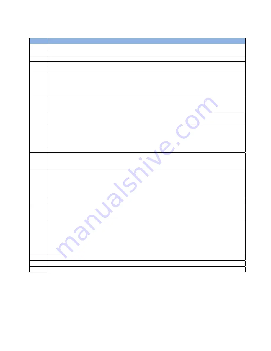
1 GROUND
2
DB2
- FIFO Data Bus Bit 2
3
DB7
- FIFO Data Bus Bit 7
4
DB5
- FIFO Data Bus Bit 5
5
DB3
- FIFO Data Bus Bit 3
6
PWREN#
- Goes low after the module is configured by USB, then high during USB
Suspend. This output can be used to control an external P-channel, logic-level MOSFET
switch. Enable the interface pull-down option when using the PWREN# pin in this way.
PWREN# should be pulled to VCCIO with 10k-Ohm resistor.
7
VCCIO
- +1.8V to +5.25V supply for the FIFO interface. Connect this pin to an external
power supply to drive out at +3.3V levels (or another voltage within the specified range),
or connect to EXTVCC (Pin 8) to drive out at the +5V CMOS level.
8
EXTVCC
- Use for applying main power (4.0 to 5.25 volts) to the module. Connect to
PORTVCC (Pin 9) if the module is to be powered by the USB port (typical configuration).
9
PORTVCC
- Power from the USB port. Connect to EXTVCC (Pin 8) if the module is to
be powered by the USB port (typical configuration). 500mA is the maximum current
available to the USB adapter and target electronics if the USB device is configured for
high power.
10 GROUND
11
RD#
- When pulled low, RD# takes the 8 data lines from a high-impedance state to the
current byte in the FIFO’s buffer. Taking RD# high returns the data pins to a high-
impedance state and prepares the next byte (if available) in the FIFO to be read.
12
WR
- When taken from a high to a low state, WR reads the 8 data lines and writes the
byte into the FIFO’s transmit buffer. Data written to the transmit buffer is sent to the host
PC within the TX buffer timeout value (default 16mS) and placed in the buffer that was
created when the USB port was opened. The FT245R allows the TX buffer timeout value
to be reprogrammed to a value between 1 and 255mS.
13
DB6
- FIFO Data Bus Bit 6
14
TXE#
- When high, do not write data into the FIFO. When low, data can be written into
the FIFO by strobing WR high, then low. During reset this signal pin is tri-state. Data is
latched into the FIFO on the falling edge of the WR pin.
15
RXF#
- When low, at least 1 byte is present in the FIFO’s receive buffer and is ready to
be read with RD#. RXF# goes high when the receive buffer is empty. During reset this
signal pin is tri-state. If the Remote Wakeup option is enabled in the internal EEPROM,
during USB Suspend Mode (PWREN#=1) RXF# becomes an input. This can be used to
wake up the USB host from Suspend Mode by strobing this pin low for a minimum of
20ms which will cause the device to request a resume on the USB bus.
16
DB1
- FIFO Data Bus Bit 1
17
DB4
- FIFO Data Bus Bit 4
18
DB0
- FIFO Data Bus Bit 0