background image

18 


APPLICATION NOTES


USING THE CONTROLLER WITHOUT BUTTONS ATTACHED 

This is very straightforward by following the steps below : 


Firstly setup the controller/display system with the buttons.  With controls attached and display system active make any 
settings for colour and image position as required then switch everything off. 


Use a jumper to close JP6 jumper, this will fix the board On. 


Refer to inverter specifications for details as to fixing brightness to a desired level, this may require a resistor, an open 
circuit or closed circuit depending on inverter. 


INVERTER CONNECTION 

There are potentially 3 issues to consider with inverter connection: 


Power 


Enable 


Brightness 

Please read the following sections for a guide to these issues. 
 

Inverter Power

: As per the table for CNB1 pin 1 is ground and pin 2 provides DC12V/ 24V DC   . This should be matched with 

the inverter specification: see table. 


CNB1 

PIN 

DESCRIPTION 

Ground 

+12VDC / 24VDC 

Remark:  For higher power inverter, more current (for 12V / 24V) can be taken from CNA1 pin 1. 
Maximum current drawn on CNA1 pin 1 and CNB1 pin 2 is 3A (24V) / 3A(12V) 
 

Enable

: This is a pin provided on some inverters for On/Off function and is used by this panel controller for VESA DPMS 

compliance. If the inverter does not have an enable pin or the enable pin is not used then DPMS will not be operational. Pin 3 
should be matched to the inverters specification for the ‘enable’ or ‘disable’ pin.   


CNB1 

PIN 

DESCRIPTION 

Enable 


Further, jumpers JB2 & JB3 should be set to match the inverters specification for the enable pin power and High or Low setting: 
see table. 
 

Ref 


Purpose 

Note 

JB2 

Inverter enable voltage 

1-2 H = 12V/24V, 2-3 H = 5V (Vcc), OPEN H = open collector 

JB3 

Inverter control 

1-2 H = On, 2-3 L = On 


Brightness

: There are various methods for brightness control and it is important to consider the specifications for the inverter 

to be used. Generally the situation is: 


Brightness can controlled by using a resistor or VR (Variable Resistor). 


Brightness controlled by adding a circuit such as PWM (Pulse Width Modulation). 


No adjustment of brightness is possible. 

CNB1 pins 4 & 5 are available for connecting to an inverter or circuit where VR control is supported.  


CNB1 

PIN 

DESCRIPTION 

VR WIP 

VR A 

 
This can then be matched with function controls (OSD switch mount) pins 3 & 4: see cable design below . 


Summary of Contents for 417100041-3

Page 1: ...ow to use the controller 9 Connectors pinouts jumpers Essential connection information 17 Controller dimensions 18 Application notes 20 Troubleshooting 21 Specifications 22 Appendix I Graphic Mode Support Table 23 Appendix II RS 232 control protocols 26 Appendix III Mapping definition 28 Appendix IV Auto Color Gain 29 Warranty Caution Limitation of Liability Trademarks 30 Contact details It is ess...

Page 2: ...ity for damage or injury caused by the use of this product It is the responsibility of the developer integrators or other user of this product to Ensure that all necessary and appropriate safety measures are taken Obtain suitable regulatory approvals as may be required Check power settings to all component parts before connection Understand the operation and connectivity requirements of this contr...

Page 3: ... pin assignment Make sure correct cable pin out to match the inverter Using wrong cable pin out may damage the inverter 7 Function Controls The following section discusses the controls required and the section on connectors provides the detail The controls are minimal On Off Backlight Brightness depends on inverter OSD 5 momentary buttons analog VR type or 8 momentary buttons digital type 8 Functi...

Page 4: ... or instability in the PC graphics output this may result in visible noise on the display Refer to graphics modes table in specifications section for supported modes Non interlaced interlaced video input is acceptable IMPORTANT Please read the Application Notes section for more information ...

Page 5: ...inverter specification and information on the jumper table to define the correct settings JA3 JA6 are used for panel voltage input read panel specification and information on the jumper table to define the correct settings 9 DVI cable Plug the DVI cable to the connector P2 on the controller board 10 VGA cable Controller Plug the VGA cable to the connector P1 on the controller board 12 Power supply...

Page 6: ...and hold SEL DN button then power on the controller Lock OSD menu Function with signal input only Press and hold MENU button for 15 seconds to enable disable lock of the OSD menu Press and hold MENU button for 15 seconds to enable disable lock of the OSD menu Direct access key for Brightness level increase under OSD menu off state Direct access key for Brightness level decrease under OSD menu off ...

Page 7: ...7500K Set the color temperature to 9300K Gamma adjustment Adjust Gamma settings 0 4 0 6 1 0 1 6 2 2 Select Gamma to 0 4 Select Gamma to 0 6 Select Gamma to 1 0 Select Gamma to 1 6 Select Gamma to 2 2 Exit Exit the OSD menu and save the settings Position Autosetup Auto adjust the positions phase frequency Yes No Frequency Adjust the image horizontal size Phase Fine tune the data sampling position a...

Page 8: ...8 Exit Exit the OSD menu Exit the OSD menu Firmware version V1 76 or up Function in ARGB mode only Items marked have sub menus Exit the OSD menu to save the setting chosen ...

Page 9: ...l control for firmware programming or RS 232 control use only JST 6 way B6B XH A Mating type XHP 6 CNA1 Auxiliary power output JST 4 way B4B XH A Mating type XHP 4 CNB1 Backlight inverter JST 5 way B5B XH A Mating type XHP 5 CNC1 Function controls JST 12 way B12B XH A Mating type XHP 12 LED1 Dual color LED connector Header pin 3x1 P1 ARGB signal input DB 15 way high density 3 row P2 DVI D signal i...

Page 10: ...light inverter on off control polarity 1 2 control signal high CCFT ON 2 3 control signal low CCFT ON JP2 Backlight control type selection 1 2 VR Digital switch mount control 3 4 Analog backlight brightness controlled by RS 232 voltage range 0 5V 5 6 Reserved JP6 Input power control Short External switch control Open Switch mount control JP7 Reserved Reserved for internal programming use Always 1 ...

Page 11: ... 4 12V 12V closed 3 5 4 6 24VDC 18V 18V closed 3 5 4 6 Please make sure the backlight inverter must support 24V supply Because CNA1 pin 1 and CNB1 pin 2 will output 24VDC if input 24VDC via PP2 JA3 JA6 location on board Please pay attention to the jumper settings on JA3 JA6 which are red in color on board ...

Page 12: ...EC NL6448BC26 09 4 c 640x480 OFF OFF ON OFF Toshiba LTA070A321F 2 800x480 ON OFF OFF ON Mitsubishi AA050MC01 3 800x480 OFF ON OFF ON NEC NL8048BC19 02 4 800x480 OFF OFF ON ON Sharp LQ070Y3LG4A 4 b 800x480 Others ON OFF OFF OFF Chunghwa CLAA070NA01CT 3 1024x600 OFF ON OFF OFF NEC NL12880BC20 02D 3 1280x800 ON ON OFF OFF NEC NL4823BC37 05 3 a 480x234 For additonal and recent added panels see ALR 140...

Page 13: ...8 GND Ground 29 TXBC Positive LVDS clock for B channel 30 TXBC Negative LVDS clock for B channel 31 GND Ground 32 GND Ground 33 VDD 3 3V 5V Panel power supply 3 3V 5V selected by JA3 JA6 34 VDD 3 3V 5V Panel power supply 3 3V 5V selected by JA3 JA6 35 VDD 3 3V 5V Panel power supply 3 3V 5V selected by JA3 JA6 36 VDD 3 3V 5V Panel power supply 3 3V 5V selected by JA3 JA6 37 NC No connection 38 VDD ...

Page 14: ... data bit G1 19 OG2 Odd data bit G2 20 OG3 Odd data bit G3 21 OG4 Odd data bit G4 22 OG5 Odd data bit G5 23 OG6 Odd data bit G6 24 OG7 Odd data bit G7 25 GND Ground 26 GND Ground 27 NC No connection 28 NC No connection 29 OB0 Odd data bit B0 30 OB1 Odd data bit B1 31 OB2 Odd data bit B2 32 OB3 Odd data bit B3 33 OB4 Odd data bit B4 34 OB5 Odd data bit B5 35 OB6 Odd data bit B6 36 OB7 Odd data bit ...

Page 15: ...ight power supply 12VDC 24V DC 3A max 3 BLCTRL Backlight On Off control signal refer to JB2 JB3 4 BVR_WIP Backlight brightness VR pin WIP 5 BVR_A Backlight brightness VR pin A CNC1 Control switch JST B12B XH A PIN SYMBOL DESCRIPTION 1 PSWIN Power button A 2 SW_ON Power button B 3 BVR_A Backlight Brightness VR pin A 4 BVR_WIP Backlight Brightness R pin WIP 5 BVR_B Backlight Brightness VR pin B 470 ...

Page 16: ...SCL DDC serial clock P2 DVI D input PIN SYMBOL DESCRIPTION 1 RX2 TMDS Data 2 2 RX2 TMDS Data 2 3 GND Digital Ground 4 NC No connection 5 NC No connection 6 DVI_DDC_CLK DDC Clock 7 DVI_DDC_DAT DDC Data 8 DVI_VS_IN Analog vertical Sync 9 RX1 TMDS Data 1 10 RX1 TMDS Data 1 11 GND Digital Ground 12 NC No connection 13 NC No connection 14 DVI_DDC_5V 5V power supply for DDC optional 15 GND Ground 5 Anal...

Page 17: ... of PCB if mounting on a metal plate we also recommend a layer of suitable insulation material is added to the mounting plate surface 10mm above the components 3 5mm around the edges Any of the holes shown above can be used for mounting the PCB they are 3 2mm in diameter CAUTION Ensure adequate insulation is provided for all areas of the PCB with special attention to high voltage parts such as the...

Page 18: ... pin 1 and CNB1 pin 2 is 3A 24V 3A 12V Enable This is a pin provided on some inverters for On Off function and is used by this panel controller for VESA DPMS compliance If the inverter does not have an enable pin or the enable pin is not used then DPMS will not be operational Pin 3 should be matched to the inverters specification for the enable or disable pin CNB1 PIN DESCRIPTION 3 Enable Further ...

Page 19: ... is handled by a relay on the controller Example for circuit design Signal description Notes 1 R1 470ohm on board 2 RPOT is an external potentiometer in line dip style that can be plugged directly into CNC1 pins 3 4 5 RPOT must be supplied installed by user 3 BVR_B Voltage tapped from top of potentiometer the node of R1 and RPOT 4 BVR_WIP Voltage tapped from wiper arm of RPOT 5 BVR_A Voltage tappe...

Page 20: ...ormally a signal splitter will not have any adverse effect Image appearance A faulty panel can have blank lines failed sections flickering or flashing display Incorrect graphics card refresh rate resolution or interlaced mode will probably cause the image to be the wrong size to scroll flicker badly or possibly even no image Incorrect jumper settings on the controller may cause everything from tot...

Page 21: ...re stored in non volatile memory Language OSD support Graphics OSD icons VESA DPMS implementation Yes Plug Play VESA DDC 1 2 b compatible Voltage output for LCD 3 3V 5V 12V 18V The current drawn for 18V panel from 24VDC power input is limited to 2A The current drawn for 3 3V 5V or 12V panel from 12V 24VDC power input is limited to 3A Input voltage 12VDC 5A max 24VDC 5A max 5 Controller power consu...

Page 22: ...e Sync SV_60 800x600 60Hz 40 000 37 879 60 317 Digital Separate Sync SV_60 800x600 60Hz 40 000 37 879 60 317 Sync On Green SV_60 800x600 60Hz 40 000 37 879 60 317 Composite Sync X_60 1024x768 60Hz 65 000 48 363 60 004 Digital Separate Sync X_60 1024x768 60Hz 65 000 48 363 60 004 Sync On Green X_60 1024x768 60Hz 65 000 48 363 60 004 Composite Sync SX_60 1280x1024 60Hz 108 63 81 60 020 Digital Separ...

Page 23: ...u button pressed Button equivalent Select down button 0xfa Select down button pressed Button equivalent Select up button 0xfb Select up button pressed Button equivalent Right button 0xfc Right button pressed Button equivalent Left button 0xfd Left button pressed Button equivalent 2 Parameter setting immediate relative reset and query Function Command Description Acknowledge if enabled Brightness c...

Page 24: ...ur temperature Range 8 0 F F Default F F Blue level for selected colour temperature 0xb6 nn r R Set the level of the blue channel for the selected colour temp value increment decrement Reset Query Blue level for selected colour temperature Range 8 0 F F Default F F OSD turn off 0xbd Turn off the OSD 1 successful Backlight brightness control 0xe0 nn r R Set backlight brightness value increment decr...

Page 25: ... Query PCBA number 0xcb 1 Read PCBA number nnnn PCBA number ALR 1400 41710 Load factory defaults 0xce Reset all parameters to factory default value 1 successful Function in ARGB mode only Hex to ASCII conversion table Hex ASCII Hex ASCII Hex ASCII Hex ASCII 0x30 0 0x41 A 0x61 a 0x2B 0x31 1 0x42 B 0x62 b 0x2D 0x32 2 0x43 C 0x63 c 0x3F 0x33 3 0x44 D 0x64 d 0x34 4 0x45 E 0x65 e 0x35 5 0x46 F 0x66 f 0...

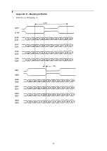
Page 26: ...26 Appendix III Mapping definition Definition of Mapping A ...

Page 27: ...27 Definition of Mapping B ...

Page 28: ...st the relative values of the RGB signals to achieve the best performance The parameters of the corrected RGB values are then stored in the controller and are unaffected by the Reset Factory Defaults function Warning If the Auto Color Gain is executed without an appropriate image being displayed then the process will set incorrect values and the display colors will be distorted If this occurs then...

Page 29: ...anties of merchantability and fitness for a particular application or purpose The stated express warranties are in lieu of all obligations or liabilities on the part of the manufacturer for damages including but not limited to special indirect consequential damages arising out of or in connection with the use of or performance of the products CAUTION Whilst care has been taken to provide as much d...

Page 30: ...iew com EUROPE Digital View Ltd 6 Marylebone Passage London W1W 8EX UK Tel 44 0 20 7631 2150 Fax 44 0 20 7631 2156 Sales uksales digitalview com USA Digital View Inc 18440 Technology Drive Building 130 Morgan Hill California 95037 USA Tel 1 408 782 7773 Fax 1 408 782 7883 Sales ussales digitalview com WEBSITE www digitalview com Specifications subject to change without notice 9th issue 24 Nov 2010...

Reviews: