Designsoft TINALab II Quick Start Manual Download Page 14


14

QUICK START 

 
If you use TINALab Spartan board together with TINA circuit simulation software and 

TINALab II High Speed Multifunction PC Instrument there is possible to develop VHDL code 
with simulation capabilities and after implementing, you can download your design and measure 
back the signals with the help of TINALab II Digital Signal Generator and Logic Analyzer. TINA 
provides code developing, simulation and measurement control with TINALab II, which does 
power supplies and signal link. 
To generate FPGA downloadable configuration file, you will need Xilinx ISE 

Webpack

TM

 software 

(

http://www.xilinx.com/ise/logic_design_prod/webpack.htm

). 

The following examples apply TINA 8 and Xilinx ISE 

Webpack

TM 

10.1.02. 


1.


Connect TINALab II with your XC2S FPGA card as described under TINALab II User 

Port on page 7. 

2.


Open the \examples\vhdl\fpga\full_add.tsc sample design. 

3.


Press the VHD button on the toolbar to enter interactive mode. 

4.


Toggle the switches to change the logic low and high levels on the input of the adder. 

Depending on the state of the inputs the outputs change state as the function of the full 
adder. 

5.


Now, create the VHDL program source for the FPGA card.  
Press  T&M > Create VHD & UCF file… Save the vhd and ucf file.  

6.


Start Xilinx ISE 

WebPACK

TM

 and create a new project (File > New project…) with the 

following settings.  
Project name: Full_Add 
Project location: [Setting Folder]\VHDL\Projects2\e_FULL_ADD_entity (See Settings 

Folder value View > Editor Options > Environment Variables.) 

Top-level source type: HDL 
Click Next. 

7.


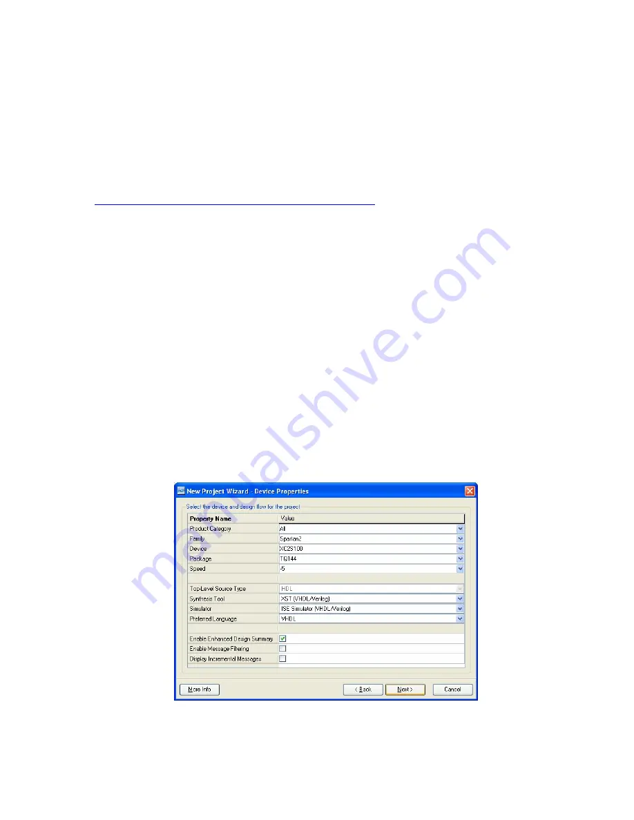
Fill the Device Properties dialog. Note, - that Device should exactly match the FPGA type 

mounted on the board. 


Click Next then Next again to skip the “Add New Source” window. 

Summary of Contents for TINALab II

Page 1: ...A Quick Start To TINALab II FPGA Development Kit 2009 www designsoftware com...

Page 2: ...2...

Page 3: ...ith the help of TINALab II Digital Signal Generator and Logic Analyzer TINA provides code developing simulation and measurement control with TINALab II which does power supplies and signal link Forty...

Page 4: ...rcuit simulator Measurement control Virtual instruments USB TINALab II High speed multifunctional PC instrument Digital Signal Generator and Logic Analyzer Xilinx ISE WebPACK Implementing FPGA Create...

Page 5: ...RTL level Simulation Design Entry schematic or VHDL Place Route Synthesis Configuration Download Virtual Instruments Digital Signal Generator Logic Analyzer TINALab Spartan II FPGA Card Results in TI...

Page 6: ...RS232 serial port J6 J7 N C J8 External power supply connector 5V J9 Multilink connector JTAG configuration link JTAG chain broker J10 PS2 port J11 VGA port JP1 Power supply and configuration jumper C...

Page 7: ...Remove connections from J9 header pin 2 6 8 10 and J3 2 Remove external power supply plug from J8 3 Open all the jumpers of JP2 Slave Serial mode 4 Close JP4 pin 2 to 3 and JP1 pin 1 to 2 5 Switch of...

Page 8: ...intercept either the ISP FLASH TDO or the FPGA TDI Set JP2 configuration mode pins in Boundary scan mode SLAVE SERIAL In serial slave mode the FPGA is configured by external configuration hardware e...

Page 9: ...de the user source clock by up to 16 NET CLK LOC P88 On board SMD oscillator Y2 NET GCK3 LOC P15 Socketed 3 3V oscillator Y1 PUSH BUTTONS The Spartan II development board design provides four push but...

Page 10: ...7 input NET switch 0 PULLUP Internal pull up resistor NET switch 1 PULLUP Internal pull up resistor NET switch 2 PULLUP Internal pull up resistor NET switch 3 PULLUP Internal pull up resistor NET swit...

Page 11: ...umeric LED display segment E NET DISPF LOC P42 4 digit numeric LED display segment F NET DISPG LOC P40 4 digit numeric LED display segment G NET DISPDP LOC P28 4 digit numeric LED display decimal poin...

Page 12: ...interface mini DIN connector J10 to either a keyboard or a mouse The FPGA receives two signals from the PS 2 interface a clock signal and a serial data stream that is synchronized with the falling ed...

Page 13: ...P74 NET DIn 11 LOC P75 NET DIn 12 LOC P65 NET DIn 13 LOC P66 NET DIn 14 LOC P60 NET DIn 15 LOC P64 The following pins can be connected to TINALab II Logic Analyzer by a ribbon cable through J1 block h...

Page 14: ...C2S FPGA card as described under TINALab II User Port on page 7 2 Open the examples vhdl fpga full_add tsc sample design 3 Press the VHD button on the toolbar to enter interactive mode 4 Toggle the sw...

Page 15: ...Rerun All WebPACKTM will synthesize and implement the circuit into a bitstream file 10 Now choose T M Download to FPGA Card in the TINA program Select the e_full_add_entity bit file from your ISE pro...

Page 16: ...Rp and Cp components are to model the TINALab II Oscilloscope Probe If we perform measurement by the instrument on the card the Probe will affect the output signal The PreScaler divides 50M to 1MHz 3...

Page 17: ...on the steps are identical with those of the previous example until creating configuration bitstream to download 6 After downloading the bit file by TINA let us measure the output signal in real Set t...

Page 18: ...ort curves button The Diagram Window will come up Copy the curves into the same diagram T Measured Simulated 0 00 25 00u 50 00u 75 00u 100 00u A 0 00 4 00 Measured Simulated TINALab FPGA Quick Start R...

Reviews: