


17
DHT-500SD
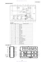
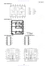
AT49F001N-70JC(ME:U3)
FAN8024BDTF(ME:U6)
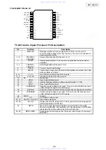
Pin Configurations
Pin Name
Function
A0 - A16
Addresses
CE
Chip Enable
OE
Output Enable
WE
Write Enable
RESET
RESET
I/O0 - I/O7
Data Inputs/Outputs
NC
No Connect
DC
Don’t Connect
5
6
7
8
9
10
11
12
13
29
28
27
26
25
24
23
22
21
A7
A6
A5
A4
A3
A2
A1
A0
I/O0
A14
A13
A8
A9
A11
OE
A10
CE
I/O7
4
3
2
1
32
31
30
14
15
16
17
18
19
20
I/O1
I/O2
G
ND
I/O3
I/O4
I/O5
I/O6
A12
A15
A16
RESET
*
VCC
WE
NC
*Note: This pin is a DC on the AT49F001N(T).
28
27
26
25
24
23
22
21
20
19
18
17
16
15
1
2
3
4
5
6
7
8
9
10
11
12
13
14
ST
BY
RE
F
IN
4
CA
P
4
.1
CA
P
4
.2
IN
3
V
CCGND
P
V
CC2
FB
4
P
G
ND2
DO3
−
DO3
+
DO4
−
DO4
+
IN
1
C
AP1
.1
C
AP1
.2
IN
2
.1
IN
2
.2
OUT
2
FB1
VC
C
P
G
ND1
DO2
−
DO2
+
DO1
−
DO1
+
P
V
CC1
-
+
-
+
1
0
K
2
0
K
7
.5
K
X2
7.5K
Loading
Driver
Actuator
Driver
-
+
10K
15K
-
+
-
+
2
0
K
1
0
K
7
.5
K
7.5K
-
+
X2
-
+
10K
25K
Sled
Driver
Actuator
Driver
PVCC2
VCC PVCC1
VCC
PVCC1
PVCC2
TSD
GND
GND
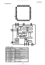
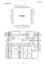
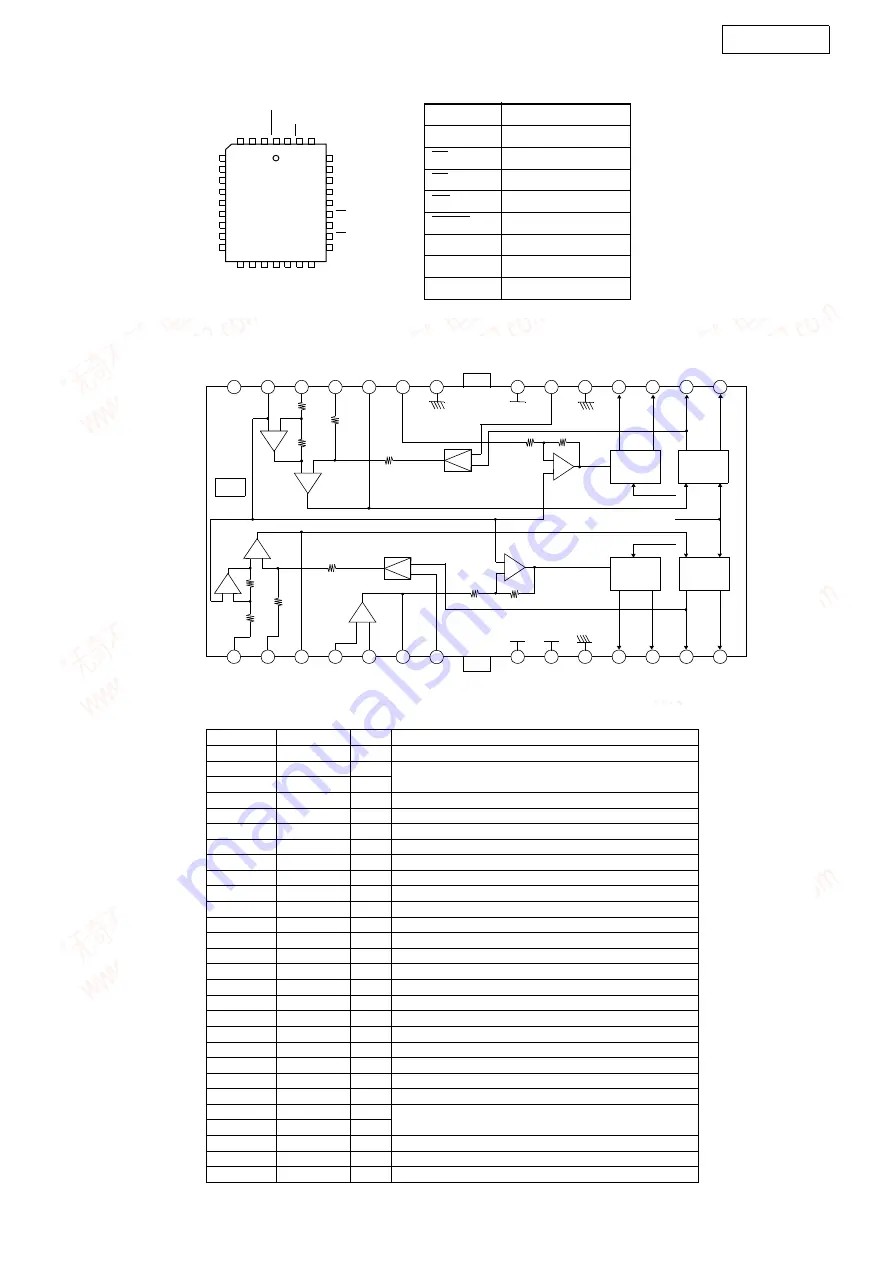
Pin Definitions
Pin Number
Pin Name
I/O
Pin Function Description
1
IN1
I
CH1 input
2
CAP1.1
-
Connection with capacitor
3
CAP1.2
-
for CH1
4
IN2.1
I
OP-AMP CH2 input(+)
5
IN2.2
I
OP-AMP CH2 input(-)
OUT2
O
OP-AMP CH2 output
FB1
I
Feedback for CH1
VCC
-
Signal Vcc
PVCC1
-
Power Supply 1
PGND1
-
Power Ground 1
DO2
−
O
Drive2 Output (-)
DO2+
O
Drive2 Output (+)
DO1
−
O
Drive1 Output (-)
DO1+
O
Drive1 Output (+)
DO4+
O
Drive4 Output (+)
DO4
−
O
Drive4 Output (-)
DO3+
O
Drive3 Output (+)
18
DO3
−
O
Drive3 Output (-)
19
PGND2
-
Power Ground 2
20
FB4
-
Feedback for CH4
21
PVCC2
-
Power Supply 2
22
VCCGND
-
Vcc ground
23
IN3
I
CH3 input
24
CAP4.2
-
Connection with capacitor
25
CAP4.1
-
for CH4
26
IN4
I
CH4 input
27
REF
I
Bias voltage input
28
STBY
I
Stand-by input
www. xiaoyu163. com
QQ 376315150
9
9
2
8
9
4
2
9
8
TEL 13942296513
9
9
2
8
9
4
2
9
8
0
5
1
5
1
3
6
7
3
Q
Q
TEL 13942296513 QQ 376315150 892498299
TEL 13942296513 QQ 376315150 892498299


