background image

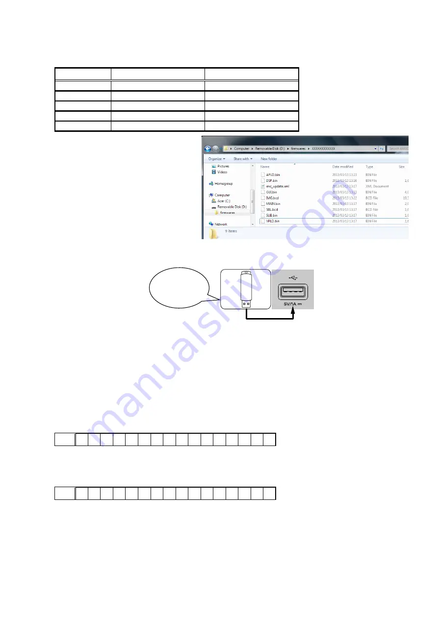
1.3.  File structure on USB Memory

Copy the update files to the USB memory with the following structure.  

USB memory root

Model Name

Model Area

Product ID

AVR-X2200WE3

North America (E3)

000100830100

AVR-X2200WE2

Europe (E2)

000100830200

AVR-X2200WJP

Japan (JP)

000100830400

AVR-X2200WE1C

China (E1C)

000100830500

AVR-S910W

North America (E3)

000100830700


+ firmwares    


  + 000100XXXXXX


+ APLD.bin


+ DSP.bin


+ enc_update.xml


+ GUI.bin


+ IMG.bcd


+ MAIN.bin


+ SBL.bcd

1.4.  Insert the USB memory into the USB port

NOTE : Remove the LAN cable from this unit when performing updates.

1.5.  Start the update

AVR-X2200W
While holding down buttons "

TUNER PRESET CH +

" and "

STATUS

" simultaneously, press the power button to turn on 

the power.
AVR-S910W
While holding down buttons "

ZONE2 SOURCE

" and "

TUNE +

" simultaneously, press the power button to turn on the 

power.

1.6.  Display during USB update

After around half minutes, display shows the following message.
Display

FLD

U S B

U p d a t e

S t a r t

1.7.  Press the "ENTER" key on the remote control unit or this unit

Then start Firmware Update.
Display

FLD

U p d a t e F i l e C h e c k

Download firmware 

in USB flash drive.

61

Summary of Contents for AVR-S910W

Page 1: ...manual with referring to the operating instructions without fail Some illustrations using in this service manual are slightly different from the actual set For purposes of improvement specifications...

Page 2: ...ode 55 7 CY920 Initialization Mode 56 JIG FOR SERVICING 57 PROCEDURE AFTER REPLACING THE MICROPROCESSOR ETC 59 FIRMWARE UPDATE PROCEDURE 60 1 Updating via USB 60 2 Updating via DPMS 69 ADJUSTMENT 76 S...

Page 3: ...you can do with this manual Search for a Ref No phrase Ctrl Shift F You can use the search function in Acrobat Reader to search for a Ref No in schematic diagrams printed wiring circuit diagrams block...

Page 4: ...Adobe Reader 9 On the Document menu click Sign Magnify schematic printed circuit board diagrams 1 Ctrl Space mouse operation Press Ctrl Space on the keyboard and drag the mouse to select the area you...

Page 5: ...en Example using Adobe Reader 9 On the Tools menu point to Select Zoom and then click Pan Zoom Window Magnify schematic printed circuit board diagrams 3 Loupe Tool function The Loupe Tool function let...

Page 6: ...tant safety parts that are indicated by the z mark on schematic diagrams and parts lists be sure to use the designated parts Be sure to mount parts and arrange the wires as they were originally placed...

Page 7: ...a part make a clear distinction between 1 and I i to avoid mis supplying 3 A part ordered without specifying its part number can not be supplied 4 Part indicated by mark is not illustrated in the expl...

Page 8: ...Personal notes 8...

Page 9: ...3 SRETEO 1 0 1 kHz for E2 E1C JP n n Wireless LAN section Network type wireless LAN standard Conforming to IEEE 802 11b Conforming to IEEE 802 11g Conforming to IEEE 802 11n Wi Fi compliant z1 Securit...

Page 10: ...34 6 1 2 165 2 1 8 54 2 11 16 69 5 8 15 6 152 6 9 16 167 9 1 4 235 11 5 16 288 13 3 8 339 3 4 19 1 1 4 32 13 9 16 344 2 3 8 60 1 3 4 45 1 3 4 45 DIMENSION FOR AVR X2200W Unit in mm Weight 20 lb 12 oz...

Page 11: ...Conforming to IEEE 802 11b Conforming to IEEE 802 11g Conforming to IEEE 802 11n Wi Fi compliant z1 Security WEP 64 bit WEP 128 bit WPA WPA2 PSK AES WPA WPA2 PSK TKIP Radio frequency 2 4 GHz No of cha...

Page 12: ...34 9 16 15 6 152 6 9 16 167 9 1 4 235 13 9 16 344 2 3 8 60 1 3 4 45 1 3 4 45 6 1 2 165 2 1 8 54 2 11 16 69 11 5 16 288 13 3 8 339 3 4 19 1 1 4 32 DIMENSION FOR AVR S910W Unit in mm Weight 20 lb 12 oz...

Page 13: ...r the service mode in step 3 repeat the procedure from step 1 Initializing the device restores the customized settings to the factory settings Write down your settings in advance and reconfigure the s...

Page 14: ...n step 3 repeat the procedure from step 1 Initializing the device restores the customized settings to the factory settings Write down your settings in advance and reconfigure the settings after initia...

Page 15: ...VIEW P 18 HDMI PCB See DISASSEMBLY 3 HDMI PCB and EXPLODED VIEW HDMI PCB Ref No of EXPLODED VIEW P 13 VIDEO PCB See DISASSEMBLY 4 VIDEO PCB and EXPLODED VIEW VIDEO PCB Ref No of EXPLODED VIEW P 19 MAI...

Page 16: ...ndicate the shooting directions of photos The photographs with no shooting direction indicated were taken from the top of the unit Photos of AVR X2200W E3 are used in this manual The viewpoint of each...

Page 17: ...PANEL ASSY Proceeding TOP COVER FRONT PANEL ASSY 1 Remove the screws 2 Remove the screws Remove the CORD HOLDERs and connector wires Remove the FFC View from the bottom x6 FFC FFC N1008 CP4400 CORD HO...

Page 18: ...e the screws 2 Remove the screws Remove the CORD HOLDERs and connector wires Remove the FFC 3 Remove the CORD HOLDERs and connector wires View from the bottom Shooting direction C Shooting direction D...

Page 19: ...ews 2 Cut the wire clamps then remove the CORD HOLDERs and connector wires Remove the FFC 3 Cut the wire clamp then remove the connector Shooting direction A x12 x25 x2 E3 ONLY x2 FFC FFC N1008 N1033...

Page 20: ...DMI PCB VIDEO PCB 1 Remove the connector 5 MAIN PCB Proceeding TOP COVER HDMI PCB VIDEO PCB MAIN PCB 1 Remove the screws 2 Remove the screws CN5000 CN5000 View from the bottom x3 x8 x2 from CP405 from...

Page 21: ...CB Proceeding TOP COVER SMPS PCB See EXPLODED VIEW for instructions on removing the SMPS PCB 7 TRANS Proceeding TOP COVER HDMI PCB TRANS See EXPLODED VIEW for instructions on removing the transformer...

Page 22: ...e number of times the power was switched on and the number of occur rences of each protection See page 52 3 User Initialization Mode TUNER PRESET CH TUNER PRESET CH Initializes backup data Settings fo...

Page 23: ...the number of occurrenc es of each protection See page 52 3 User Initialization Mode TUNER PRESET CH TUNER PRESET CH Initializes backup data Settings for the Installer Setup are not initialized 4 Fac...

Page 24: ...Firmware Package Version e Main com r Main 1st Boot Loader t DSP ROM y Audio PLD u GUI SFLASH i Ethernet 1st Boot Loader Hardware ID o Ethernet 2nd Boot Loader Rhapsody Flag Q0 Ethernet IMAGE Q1 Ethe...

Page 25: ...er Rhapsody Flag FLD E t h e r n e t S B L Press STATUS button FLD B 0 A Q0 Ethernet IMAGE FLD E t h e r n e t I M G Press STATUS button FLD I Q1 Ethernet MAC ADDRESS information FLD N E T M A C A d d...

Page 26: ...U1026 or U1028 1029 is faulty During the initial setting of i p Scaler ADV8003 there is not the reply of the Loopback Test result of the DDR memory I P S C A L E R E R R 0 2 e GUI Serial Flash NG If...

Page 27: ...d this 12 digit version information are written in the Service Information General Firmware Version XXXX XXXX XXXX GUI Image Main Sub X X 3 8 Info display 1 2 0 0 8 3 8 2 6 0 7 3 DSP X X X 2 A PLD X X...

Page 28: ...de The information shown on the display switches each time the TUNER PRESET CH button is pressed Press the STATUS button to set the currently displayed mode and restart the device The setting with is...

Page 29: ...switches each time the TUNER PRESET CH button is pressed Press the STATUS button to set the currently displayed mode and restart the device q FLD 1 S E R V I C E C H E C K Service Path Check Mode The...

Page 30: ...nt L R b The input source can be switched to any source except CBL SAT 2 DIGITAL MAIN A 0 2 D I G I T A L Input Source CBL SAT Input Mode DIGITAL fixed Sound mode MULTI CH STEREO Amp assign Surround B...

Page 31: ...I P A S S Input Source CBL SAT Video Convert IP Scaler OFF All sources MAIN ZONE ON ZONE2 OFF HDMI input MAIN function HDMI output MAIN b The input source can be switched to any source except CBL SAT...

Page 32: ..._SL EXT_SW ANA_FR EXT_FR DSP_C DSP_FL DSP_FL DSP_SW DSP_C DSP_SL SBR SBL SBR SW2 SW1 FR FL H P L H P R AVR_S910 EXCEPT PREOUT 7 1CH EXT IN OTHER AVR1 ONLY OTHER AVR1 ONLY OTHER AVR1 ONLY SBR FR B FR H...

Page 33: ...NET USB_MCK SW2_MCLK SW2_SD0 SW2_SD2 SW2_SD3_SPDIF SW2_BCLK SW1_LRCK SW1_SD1 DIRRXSPDIF IN A TMDS SLRCK DATADIR1 64FSDIR1 DIRABCKI DIRALRCKI IN D TMDS Z2_DAC_BCLK Z2_DAC_DATA DAC_FS DACDATAC DACDATAS...

Page 34: ...NA_FR EXT_FR DSP_C DSP_FL DSP_FL DSP_SW DSP_C DSP_SL SBR SBL SBR SW2 SW1 FR FL H P L H P R AVR_S910 EXCEPT PREOUT 7 1CH EXT IN OTHER AVR1 ONLY OTHER AVR1 ONLY OTHER AVR1 ONLY SBR FR B FR H BI AMP ZONE...

Page 35: ...NET USB_MCK SW2_MCLK SW2_SD0 SW2_SD2 SW2_SD3_SPDIF SW2_BCLK SW1_LRCK SW1_SD1 DIRRXSPDIF IN A TMDS SLRCK DATADIR1 64FSDIR1 DIRABCKI DIRALRCKI IN D TMDS Z2_DAC_BCLK Z2_DAC_DATA DAC_FS DACDATAC DACDATAS...

Page 36: ...NA_FR EXT_FR DSP_C DSP_FL DSP_FL DSP_SW DSP_C DSP_SL SBR SBL SBR SW2 SW1 FR FL H P L H P R AVR_S910 EXCEPT PREOUT 7 1CH EXT IN OTHER AVR1 ONLY OTHER AVR1 ONLY OTHER AVR1 ONLY SBR FR B FR H BI AMP ZONE...

Page 37: ...NET USB_MCK SW2_MCLK SW2_SD0 SW2_SD2 SW2_SD3_SPDIF SW2_BCLK SW1_LRCK SW1_SD1 DIRRXSPDIF IN A TMDS SLRCK DATADIR1 64FSDIR1 DIRABCKI DIRALRCKI IN D TMDS Z2_DAC_BCLK Z2_DAC_DATA DAC_FS DACDATAC DACDATAS...

Page 38: ...NA_FR EXT_FR DSP_C DSP_FL DSP_FL DSP_SW DSP_C DSP_SL SBR SBL SBR SW2 SW1 FR FL H P L H P R AVR_S910 EXCEPT PREOUT 7 1CH EXT IN OTHER AVR1 ONLY OTHER AVR1 ONLY OTHER AVR1 ONLY SBR FR B FR H BI AMP ZONE...

Page 39: ...NET USB_MCK SW2_MCLK SW2_SD0 SW2_SD2 SW2_SD3_SPDIF SW2_BCLK SW1_LRCK SW1_SD1 DIRRXSPDIF IN A TMDS SLRCK DATADIR1 64FSDIR1 DIRABCKI DIRALRCKI IN D TMDS Z2_DAC_BCLK Z2_DAC_DATA DAC_FS DACDATAC DACDATAS...

Page 40: ...NA_FR EXT_FR DSP_C DSP_FL DSP_FL DSP_SW DSP_C DSP_SL SBR SBL SBR SW2 SW1 FR FL H P L H P R AVR_S910 EXCEPT PREOUT 7 1CH EXT IN OTHER AVR1 ONLY OTHER AVR1 ONLY OTHER AVR1 ONLY SBR FR B FR H BI AMP ZONE...

Page 41: ...NA_FR EXT_FR DSP_C DSP_FL DSP_FL DSP_SW DSP_C DSP_SL SBR SBL SBR SW2 SW1 FR FL H P L H P R AVR_S910 EXCEPT PREOUT 7 1CH EXT IN OTHER AVR1 ONLY OTHER AVR1 ONLY OTHER AVR1 ONLY SBR FR B FR H BI AMP ZONE...

Page 42: ...UTPUT COMP2 Cr COMP2 Cb IN1 CBL SAT COMP1 Cr COMP1 Cb COMP1 Y FRONT HDMI INPUT SELECT TMDS IN HDMI2 0 RX MN864788 2 2 4 INPUTS A3R12E40CBF HDMI i p Scaler_TX_OSD ADV8003 8B AD55 058Z 0 OSD MX25L12835F...

Page 43: ...UTPUT COMP2 Cr COMP2 Cb IN1 CBL SAT COMP1 Cr COMP1 Cb COMP1 Y FRONT HDMI INPUT SELECT TMDS IN HDMI2 0 RX MN864788 2 2 4 INPUTS A3R12E40CBF HDMI i p Scaler_TX_OSD ADV8003 8B AD55 058Z 0 OSD MX25L12835F...

Page 44: ...UTPUT COMP2 Cr COMP2 Cb IN1 CBL SAT COMP1 Cr COMP1 Cb COMP1 Y FRONT HDMI INPUT SELECT TMDS IN HDMI2 0 RX MN864788 2 2 4 INPUTS A3R12E40CBF HDMI i p Scaler_TX_OSD ADV8003 8B AD55 058Z 0 OSD MX25L12835F...

Page 45: ...UT COMP2 Cr COMP2 Cb IN1 CBL SAT COMP1 Cr COMP1 Cb COMP1 Y FRONT HDMI INPUT SELECT TMDS IN HDMI2 0 RX MN864788 2 2 4 INPUTS A3R12E40CBF HDMI i p Scaler_TX_OSD ADV8003 8B AD55 058Z 0 OSD MX25L12835FMI...

Page 46: ...NET USB_MCK SW2_MCLK SW2_SD0 SW2_SD2 SW2_SD3_SPDIF SW2_BCLK SW1_LRCK SW1_SD1 DIRRXSPDIF IN A TMDS SLRCK DATADIR1 64FSDIR1 DIRABCKI DIRALRCKI IN D TMDS Z2_DAC_BCLK Z2_DAC_DATA DAC_FS DACDATAC DACDATAS...

Page 47: ...NA_FR EXT_FR DSP_C DSP_FL DSP_FL DSP_SW DSP_C DSP_SL SBR SBL SBR SW2 SW1 FR FL H P L H P R AVR_S910 EXCEPT PREOUT 7 1CH EXT IN OTHER AVR1 ONLY OTHER AVR1 ONLY OTHER AVR1 ONLY SBR FR B FR H BI AMP ZONE...

Page 48: ...NET USB_MCK SW2_MCLK SW2_SD0 SW2_SD2 SW2_SD3_SPDIF SW2_BCLK SW1_LRCK SW1_SD1 DIRRXSPDIF IN A TMDS SLRCK DATADIR1 64FSDIR1 DIRABCKI DIRALRCKI IN D TMDS Z2_DAC_BCLK Z2_DAC_DATA DAC_FS DACDATAC DACDATAS...

Page 49: ...UTPUT COMP2 Cr COMP2 Cb IN1 CBL SAT COMP1 Cr COMP1 Cb COMP1 Y FRONT HDMI INPUT SELECT TMDS IN HDMI2 0 RX MN864788 2 2 4 INPUTS A3R12E40CBF HDMI i p Scaler_TX_OSD ADV8003 8B AD55 058Z 0 OSD MX25L12835F...

Page 50: ...impedance outside the rating were connected If the power is turned on in the abnormal state protection is activated after around 6 seconds and the power is turned off c DC if the last protection is D...

Page 51: ...unit Warning Displays by POWER LED If the power is turned off while a protection is being detected the POWER LED flashes in red to warn you depending on the protection status as follows a ASO DC prot...

Page 52: ...he power Select the 4 OP INFO using the TUNER PRESET CH button then press the STATUS button to confirm 3 6 3 Operations Press the STATUS button after starting up this device in Operation Info mode The...

Page 53: ...but ton to turn on the power Select the 5 TUNER FRQ SET using the TUNER PRESET CH button then press the STATUS button to confirm 3 7 3 Displays Start up this unit in TUNER STEP mode select the desired...

Page 54: ...Operations 1 When Remote ID Setup mode is activated the following message is displayed FLD R E M O T E I D 2 Press the desired QUICK SELECT 1 4 button Button Display QUICK SELECT 1 R E M O T E I D 1...

Page 55: ...ay message after the following is displayed FLD P r o t e c t i o n P a s s This is displayed for 5 seconds before returning to the normal display 6 CY920 Reboot Mode 6 1 Actions The CY920 is restarte...

Page 56: ...on hold down buttons ZONE2 SOURCE and DIMMER for at least 3 seconds AVR S910W While the power is on hold down buttons TUNER PRESET CH and TUNE for at least 3 seconds Initializing Display FLD I n i t...

Page 57: ...ctions may cause malfunction Connection of Jig for HDMI PCB Items to Be Prepared 8U 110084S EXTENSION UNIT KIT 1Sets 8U 110136S EXTENSION UNIT KIT 1Sets Insulation sheet Not supplied 2 sheets Ground l...

Page 58: ...xpansion cables Board to Board Connections No Pin Ref No PCB Ref No PCB q 15pin CP4200 INPUT N1020 HDMI w 27pin CP4205 INPUT N1016 HDMI e 23pin CP4201 INPUT N1014 HDMI r 25pin CP3401 FRONT CNT N1039 H...

Page 59: ...display if the DIGITAL PCB or the CY920 is replaced as this results in the version of the INTERNAL ROM differing from that of the EXTERNAL ROM In this case see Update Procedure in the Event of a CY92...

Page 60: ...of this unit using a USB cable Do not use an extension cable when connecting the USB unit If a USB memory device cannot be updated replace it with a different USB memory device and perform the update...

Page 61: ...mory into the USB port NOTE Remove the LAN cable from this unit when performing updates 1 5 Start the update AVR X2200W While holding down buttons TUNER PRESET CH and STATUS simultaneously press the p...

Page 62: ...aneously insert the AC plug to turn the power on AVR S910W While holding down buttons the ZONE2 SOURCE and TUNE buttons simultaneously insert the AC plug to turn the power on 1 9 3 The firmware update...

Page 63: ...d 0 B No Firmware File for Firmware Download Make sure that the Firmware File is in the USB memory 0D C o n n e c t i o n F a i l 0 D Received value with the invalid Package Version This unit automati...

Page 64: ...n n e c t i o n F a i l 2 5 Failed to transit to SBL Mode This unit automatically retries the request several times Wait until the Display stops If the Display stops at the Error display press and hol...

Page 65: ...tically retries the request several times Wait until the Display stops If the Display stops at the Error display press and hold the Power operation button for 5 seconds 56 C o n n e c t i o n F a i l...

Page 66: ...al times Wait until the Display stops If the Display stops at the Error display press and hold the Power operation button for 5 seconds 81 U p d a t i n g f a i l 8 1 Block Erase failed in Read after...

Page 67: ...or Firmware Download This unit automatically retries the request several times Wait until the Display stops If the Display stops at the Error display press and hold the Power operation button for 5 se...

Page 68: ...4 Audio PLD L1 A P L D m i n 50 52 54 57 5A 64 DSP L1 D S P m i n 50 52 54 57 5A 64 GUI Serial Flash L1 G U I m i n 50 52 54 57 5A 62 64 80 86 CY920 second Boot Loader L1 E S B L m i n A2 A4 A6 A7 AE...

Page 69: ...talled press the SETUP button to exit the menu 4 Select Start using the cursor buttons and then press ENTER The power display lights in red and the GUI screen display disappears during the update The...

Page 70: ...nt that has little network load 08 C o n n e c t i o n F a i l 0 8 Error notification received while requesting the Firmware Info Check the network connection Carry out the update in an environment th...

Page 71: ...little network load 22 L o g i n f a i l e d 2 2 DPMS login incorrect notification after SBL Initialize the unit and try updating again Carry out the update in an environment that has little network...

Page 72: ...i l e d 5 0 DPMS login incorrect notification Carry out the update in an environment that has little network load 51 S e r v e r i s b u s y 5 1 DPMS congestion notification Carry out the update in an...

Page 73: ...t i n g f a i l 6 2 Failed to start up Sub in Power On sequence during Update Turn off and on the power Updating starts automatically 80 U p d a t i n g f a i l 8 0 Write Enable Latch Bit not set in R...

Page 74: ...rmware Down load Turn off and on the power Updating starts automatically Carry out the update in an environment that has little network load AF D o w n l o a d f a i l A F Error Server Busy notificati...

Page 75: ...A 62 Audio PLD L1 A P L D m i n 50 52 54 58 5A 62 DSP L1 D S P 1 m i n 50 52 54 58 5A 62 GUI Serial Flash L1 G U I m i n 50 52 54 58 5A 62 80 86 CY920 second Boot Loader L1 E S B L m i n A0 A4 A6 A7 A...

Page 76: ...h TP402 CENTER ch TP403 SURROUND Lch TP404 SURROUND Rch TP405 SURROUND BACK Lch TP406 SURROUND BACK Rch TP407 3 Connect the power cord to an outlet Next press the power button to turn on the power 4 S...

Page 77: ...ame S D D D D D D D D D Matrix S D D D D D D D D D Virtual S D z1 A signal for each channel contained in an input signal is output as audio z2 Audio is not output when Speaker Config Surr Back in the...

Page 78: ...z1 This item can be selected when a Dolby Digital Dolby Digital Plus Dolby TrueHD or Dolby Atmos signal is played z2 This item can be selected when a Dolby TrueHD Dolby Digital or DTS signal is playe...

Page 79: ...S Original sound mode Multi Ch Stereo S S S S S S S S S S S S S S Rock Arena S S S S S S S S S S Sz10 S S S Jazz Club S S S S S S S S S S Sz10 S S S Mono Movie S S S S S S S S S S Sz10 S S S Video Gam...

Page 80: ...faulty parts To 3 5 Protection History Display Mode See page 50 Are there any parts not fully connected into the connec tors that connect the PCBs Is DC5V output even when the connector N1033 supplyin...

Page 81: ...R1384 R1438 R1800 R1805 C1302 C1307 L1070 R2040 R2045 R1389 R1388 R1387 R1386 C2146 C2157 C1198 C1907 C1913 C1916 C2089 C2105 D1087 D1088 L1018 R1946 C1172 C1777 N1009 R1207 R1209 R2052 C1730 L1144 R1...

Page 82: ...ignal be confirmed at the follow ing points HDMI PCB V R2092 COMPONENT Y R2089 COMPONENT Cb R2091 COMPONENT Cr R2090 Check the connection between the boards Input CVBS Check B Input COPONENT Check C O...

Page 83: ...the FRONT CONNECTOR PCB and the VIDEO PCB Check the soldering of CP3401 and CP5000 on the FRONT CONNECTOR PCB Check the soldering of CN5000 on the VIDEO PCB Check the IC5001 power voltage and check th...

Page 84: ...nd the VIDEO PCB Check the soldering of CP3401 and CP5000 on the FRONT CONNECTOR PCB Check the soldering of CN5000 on the VIDEO PCB Check the soldering of JACK5001 on the VIDEO PCB Extend the HDMI PCB...

Page 85: ...fluorescent display lit Proceed to YES when using a Blu ray DVD player produced by other manufactures 10 Is sound output from the speaker terminal of this unit when the power of the TV is turned off...

Page 86: ...tion manual of the TV and check the input setting The TV is faulty Check the circuits around the IP SCALER U1026 HDMI PCB and DDR2 U1028 U1029 If there appear to be no problems U1026 or U1028 1029 is...

Page 87: ...Legacy PCM or DolbyDigital or dts CHECK4 INPUT SURROND MODE SOURCE Audio output OK HDMI Legacy PCM2ch or DolbyDigital or dts CHECK6 INPUT Connect AVR s connected in HDMI audio out put OK HDMI This un...

Page 88: ...mer potentiometer between the base of the power transistor open 1 k Are any other transistors faulty Are any other resistors faulty Turn on the power and check that the voltage of each part is correct...

Page 89: ...INPUT PCB CN4006 Is there an audio signal in INPUT PCB CN401 Reconnect the connectors correctly If the malfunctioning channel and function can be identified check the correspond ing signal path Repai...

Page 90: ...settings correctly Check that there are no connection restrictions by MAC addresses etc NO NO NO 5 Network Bluetooth USB 5 1 Cannot connect to the network Is the LAN cable correctly inserted Insert t...

Page 91: ...U1018 uCOM 132 pin Hi Is E_POWER3 U1018 uCOM 134 pin Hi Is E_POWER4 U1018 uCOM 132 pin Hi Is E_POWER2 U1018 uCOM 133 pin Hi The circuit of E_POWER1 between U1018 and Q1071 are faulty The circuit of E...

Page 92: ...rted correctly into CY920 Is the Bluetooth device compatible with the A2DP profile Is the Bluetooth function enabled on the Bluetooth device Connect the Wi Fi BT antenna cable correctly Use a device t...

Page 93: ...d between pin 1 and pin 4 of CP4406 USB Connector on USB PCB The USB signal circuit between CY920 and CP4406 of the USB PCB are faulty Check the U1073 DSP AUDIO circuit and the circuits thereafter Are...

Page 94: ...33 C1612 R1707 C2138 C2102 R1683 D1077 D1078 D1079 D1080 D1081 D1082 D1083 D1084 D1132 D1133 L1062 L1120 C2055 R1897 X1007 C1680 Q1055 C2171 C2180 C2185 K1002 N1010 R2058 R2062 R2069 R2072 U1007 U1008...

Page 95: ...he PCB Check the damaged parts Replace the damaged part Replace the damaged part Is the fuse F4140 functioning proper ly Are there any short circuits caused by the soldering on the PCB Are any parts d...

Page 96: ...0v 0 01 250v C4148 10K R4152 ZJ12B ZD4162 ZJ12B ZD4163 D4146 1N4007 D4147 AP01C V1 ZD4156 ZJ22B ZD4157 ZJ22B ZD4154 ZJ22B ZD4152 ZJ22B ZD4153 ZJ22B ZD4148 ZJ39B ZD4149 ZJ39B KTC3198G TR4142 R4156 4K7...

Page 97: ...R1150 R1151 R1674 R1676 R1677 R1170 C1766 L1139 L1110 C1764 C1775 R1814 R1815 R2030 R2035 C1750 L1111 C1749 R1793 R1810 R2007 R2012 C1195 D1085 D1086 L1017 C1853 C1839 C2162 C2151 C2137 D1137 R1948 R...

Page 98: ...SIGNAL LEVEL DOLBY LIMIT LEVEL ALLch 3dBFS GAIN setting of MASTER VOL 00dB SW YES DIGITAL 2 0dB 2 0dB SW YES ANALOG 2 0dB 3 5dB 1 5dB SW NONE DIGITAL 2 0dB 12dB 10 0dB SW NONE ANALOG 2 0dB 12dB 3 5dB...

Page 99: ...R S910W X2200W LEVEL DIAGRAM CENTER ch 2dB 0dBFS 10dBFS 20dBFS 30dBFS 40dBFS 20dBFS DIG IN PCM or DD Config1 26 5dBFS A D IN 200mV 30dB SP OUT 4 48Vrms 8 29dB MAX SIGNAL LEVEL DOLBY LIMIT LEVEL ALLch...

Page 100: ...DIAGRAM SUBWOOFER ch 0dBFS 10dBFS 20dBFS 30dBFS 40dBFS 200mV 30dB MAX SIGNAL LEVEL 9 5dB 2 20 6 12dB Config1 DOLBY LIMIT LEVEL ALLch 3dBFS 50dBFS 40dBFS DIG IN DD Config1 INPUT 30dBFS DD LFE PREOUT 31...

Page 101: ...B 30dB 40dB 10dB EXT IN 0dBFS 1 41Vrms 2dB 0dBFS 10dBFS 20dBFS 30dBFS 40dBFS 20dBFS DIG IN PCM or DD Config1 26 5dBFS A D IN 200mV 30dB SP OUT 4 48Vrms 8 29dB MAX SIGNAL LEVEL DOLBY LIMIT LEVEL ALLch...

Page 102: ...A D IN 200mV 30dB SP OUT 4 48Vrms 8 26dB 2 3 6 7dB NON CLICP MAX SIGNAL LEVEL 4 0Vrms Config2 DOLBY LIMIT LEVEL 1 41Vrms ALLch 3dBFS 3dB 26dBFS DIG IN DD EX Config1 2 3 1dB DOLBY LIMIT LEVEL 1 41Vrms...

Page 103: ...10dB LINE IN 0dBFS 2 0Vrms PREOUT 0dBFS 10dBFS 20dBFS 30dBFS 40dBFS 20dBFS DIG IN PCM5100 200mV MAX SIGNAL LEVEL 2 00Vrms SPEAKER 30dB SP OUT D A from DA SB ch TO MAIN from F ch NET USB DAC BD34704 Z...

Page 104: ...L EXT_SW ANA_FR EXT_FR DSP_C DSP_FL DSP_FL DSP_SW DSP_C DSP_SL SBR SBL SBR SW2 SW1 FR FL H P L H P R AVR_S910 EXCEPT PREOUT 7 1CH EXT IN OTHER AVR1 ONLY OTHER AVR1 ONLY OTHER AVR1 ONLY SBR FR B FR H B...

Page 105: ...UT1 NET USB_MCK SW2_MCLK SW2_SD0 SW2_SD2 SW2_SD3_SPDIF SW2_BCLK SW1_LRCK SW1_SD1 DIRRXSPDIF IN A TMDS SLRCK DATADIR1 64FSDIR1 DIRABCKI DIRALRCKI IN D TMDS Z2_DAC_BCLK Z2_DAC_DATA DAC_FS DACDATAC DACDA...

Page 106: ...S OUTPUT COMP2 Cr COMP2 Cb IN1 CBL SAT COMP1 Cr COMP1 Cb COMP1 Y FRONT HDMI INPUT SELECT TMDS IN HDMI2 0 RX MN864788 2 2 4 INPUTS A3R12E40CBF HDMI i p Scaler_TX_OSD ADV8003 8B AD55 058Z 0 OSD MX25L128...

Page 107: ...POWER DIAGRAM S2 8V 8V MAIN TRANS S1 AMP B MAIN PWR ON VCC DIAGRAM AC CORD 107...

Page 108: ...E_OUT PCB SR ONLY H P PCB FRONT PCB SPK PCB VIDEO PCB AUDIO IN PCB AVR ONLY FRONT CNT PCB HDMI PCB USB PCB INPUT PCB CY920 MODULE HDAM PCB OTHER AVR1 ONLY TUNER PACK FUNCTION PCB 7CH AMP PCB VOLUME PC...

Page 109: ...IN4_DET IN5 5V IN5 G F G J IN6 5V IN6 DDCSDA I 27MHZ SPI_MI SPI_CS SPI_MO AVSDA AVSCL I DDCSDA IN7 IN7 DDCSCK IN7_DET J 3 3V J K K 2 DGND 5 D5 2V 4 D5 2V E_POWER2 1 DSP1OUTFS DSP1OUT64FS 39 24 576MHZ...

Page 110: ...2036 R2070 R2073 R4259 R5340 U1053 SAT Cr SAT Cb C OUT RC_IN KILLIR D5V MX RC_OUT V AUX D MGND CVBS D MGND VDICB VDIPY D MGND VDICR COMPONENT SW2 V_INC V_INB V_INA COMPONENT SW1 V 5V VGND V 5V V 5V VG...

Page 111: ...3 J555 R641 R651 ZD417 C491 J542 R628 R632 R708 C486 Q472 R645 Q471 R650 D431 R657 R634 C484 C488 C494 J575 R647 R674 CP405 J548 J563 JP546 R670 R678 Q474 R659 TP406 R667 VR407 VR417 C503 C510 J579 J5...

Page 112: ...0 F4001 T6 3AL 250 V JACK4003 JACK4004 470 50 10 20 2200 25 TRIGER MODEL ONLY F4000 T6 3AL 250 V MAIN B D MP C4028 J4028 R4070 R4008 C4016 J4114 J4117 D4010 J4024 J4096 J4094 J4022 J4020 J4019 R4018 J...

Page 113: ...J4507 J4554 J4535 J4488 J4448 J4484 J4493 J4479 J4528 J4451 J4460 ZD4406 R4461 J4514 R4458 J4513 J4481 Q4404 SW4418 SW4421 J4437 J4480 J4508 C4421 J4482 LED4401 RMC4400 CP4401 CP4400 C4432 SW4415 C447...

Page 114: ...R4150 ZD4156 J4153 J4156 C4142 CN4141 J4154 D4148 R4140 J4157 D4150 R4149 R4164 D4141 R4141 D4145 Pb ZD4160 D4142 ZD4151 D4144 ZD4153 BKT4141 R4153 C4155 ZD4158 D4147 C4153 FC4141B FC4141A CP4140 R415...

Page 115: ...X1_2 RX1_DDCDA RX1_C RX1_C RX1_5V RXF_2 RXF_0 RXF_1 RXF_DDCCL TXEN 100N K C1089 D1024 OPEN R1097 0 RX3_5V R1095 OPEN C1077 10P 1608 RX2_DDCCL RX3_DDCCL C1220 100N K RX3_0 RX3_1 C1222 100N K RX2_1 RX2_...

Page 116: ...107 100N K C1109 100N K SW2_SD2 SW2_SD0 SW2_MCLK SW2_LRCK AVDD33TX_1 VDD11_2 VDD33_2 AVDD33RX_1 C1183 4 7U K 1608 CB05YTYH221 L1019 WS_OPEN C1092 4 7U K 1608 P3_DDCCL P3_C P3_D1 P3_D0 P2_DDCCL P2_C P2...

Page 117: ...30 24 26 22 18 14 10 6 2 61 57 53 49 41 45 37 33 19 15 11 7 3 62 58 54 50 42 46 38 34 20 16 12 8 4 XINYA S1210 U1007 1 2 4 6 3 5 7 N1009 1 0 16 7PB 2 R1268 33 INT_FLASH_CS R1267 33 FLASH_DIN R1265 33...

Page 118: ...Y_HIB RC_OUT KEY2 FIL_CTRL R1369 33K C1286 100N K C1287 100N K KEY1 C1289 10N K R1370 18K DC_PROT SB_RLY M3 3V C1291 OPEN R1352 OPEN THER_PROTB ASO_PROT R1373 OPEN R1355 18K MIC_DET C1293 10N K R1356...

Page 119: ...RXD_MI232O DA 7V DA 7V PRE_Z2_MUTE TU_RST ST DA 5V MIC TU_SDIO SDA KEY2 ISEL_B A_ 8V DA_ 5V MUTE_Z2 DAGND MIC_IN RETGND DAGND DAGND DAGND DAGND DAGND DAC_SR DAC_SL DAGND DAC_C DAC_FR DAGND FLRST GRN_...

Page 120: ...TU_SEN 33 R1471 33 R1473 0 R1474 R1475 33 H P_DET M3 3V VIN_B UB EMLE TDI RXD UB AEXP_DATA AEXP_OE CEC_IN AVSCL DSP1MISO UB DSP1CS DSP1RST TCK NC R1460 4K7 R1462 4K7 R1464 4K7 R1458 4K7 R1457 4K7 STB...

Page 121: ...C1391S OPEN R1557S RX_2 R1557 OPEN 1N K C1395S OPEN C1397S OPEN C1400S OPEN C1398S C1388 10N K R1561 0 DDC_SDA C1382S OPEN C1380S 10U K 2012 10U K 2012 C1380 C1382 OPEN 2012 C1384S OPEN C1384 OPEN 201...

Page 122: ...SD_D15 OTHER AVR2 AVR X2200 3K3 R2102 DSP_DBCK DSP_DBDA DSP_BUSY DSP1FLAG0 C1452 100N K C1440 100N K SD_A5 SD_A7 SD_A9 SD_A12 DSP1SDCLK_IN 47 4 AR R2193 SD_D8 SD_D9 SD_D10 CB05YTYH221 L1130 R1647 3K3...

Page 123: ...OPEN 2012 C1548 100N K C1550 OPEN L1042 CB05YTYH221 33P J C1616 100N K C1614 33 R1667 33 R1668 4K7 R1652 4K7 R1637 4K7 R1640 1K R1684 0 R1680 10K R1678 C1610 12N K 1608 OPEN R1662 C1607 150N K 1608 C1...

Page 124: ...DR_TXDQ12 DR_TXDQ14 DDR_1 8V DGND DDR2 DDR2 DR_TXDQS2 DR_TXDQSB2 DDR2 DDR2 DDR2 DR_TXDM3 DR_TXDQ20 DR_TXDQ22 DR_TXDQ24 DR_TXDQ26 DDR_1 8V DDR2 DDR2 DR_TXDQ28 DR_TXDQ30 DGND DDR1 DDR1 DDR1 DDR1 DDR1 DD...

Page 125: ...100K R2040 100K R1995 100K R2003 100K MP2143DJ U1072 1UH DD1255AS 1RON L1146 MP2143DJ U1070 1UH DD1255AS 1RON L1144 MP2143DJ U1065 1UH DD1255AS 1RON L1139 1UH DD1255AS 1RON L1137 200K D 1608 R2063 200...

Page 126: ...C1991 4 7U K 1608 C1980 4 7U K 1608 C1992 4 7U K 1608 1M R1893 TX_HINT R2128 10K R2130 47K R2145 10K HSDA C2095 100N K C2096 100N K 51 D 1608 R1888 1 4 2 3 R1990 0 2 1 4 2 3 R1984 0 2 1 4 2 3 R1987 O...

Page 127: ...N C2078 100N K SLRCK PCM9211_INTO DIRABCKI DIRADATAI FSDIR1 256FSDIR1 DIRRXSPDIF ARCSPDIF DAC_ZERO_MUTE Z2_DAC_BCLK Z2_DAC_LRCK DACFS 100N K C2069 100N K C2066 33 R1942 33 R1931 DATAC DGND DV3 3V DGND...

Page 128: ...R2033 1K R2027 33 C2159 1U K 1608 C2149 10UF 16V MVG R2082 100 1608 R2069 100 1608 R2062 100 1608 R2058 100 1608 R2047 100 1608 R2038 100 1608 R2034 100 1608 R2021 100 1608 R2013 100 1608 R2002 100 16...

Page 129: ...C2242 100N K C2282 100N K C2283 10N K C2244 10N K C2246 10N K C2248 100N K C2250 10N K C2285 10N K C2287 10N K C2288 10N K C2289 10N K C2290 100N K C2303 10N K C2304 4 7U K 1608 C2305 10N K C2252 100...

Page 130: ...8V TU_SEN TUNERR TUNERL AGND AGND AGND AGND AGND AGND O X E3 O E2 E1C K X X AGND AGND AGND AGND AGND AGND AGND AGND AGND PREMUTE_F R2047 15K R2058 15K R2010 15K R2017 15K C2182 CH 330P 11K R2076 R2083...

Page 131: ...V 5V VAGND VDICR V INB VDIPY CVBS VDICB OPEN C5033 1 50 C5023 R5029 OPEN R5039 75 C5006 OPEN 68P C5009 R5071 10K R5070 10K R5069 10K 100N K C5013 100 10 C5011 CN5000 CN5003 JACK5002 CR2_IN Y1_IN C500...

Page 132: ...OPEN C5046 VGND TRG 15V 8V_IN 5V_IN 5V_IN VAGND D MGND D MGND D MGND 8V_IN RET_GND COMPONENT SW2 V IN B D MGND V IN C D MGND COMPONENT_SW1 RLY_H P RLY_C S COMPONENT SW1 AMPSIG_DET PREMUTE_SB H P_R V...

Page 133: ...K R5737 18K R5740 47 C5662 OPEN 4700N K C5663 100N K C5679 FRONT_IRIN R5711 OPEN 2W M3 3V 33K R5720 OPEN 2W R5710 R5718 100 C5678 100N K D5617 LBAS16HT1G R5719 100 RT1P141C Q5625 Q5626 RT1P141C Q5630...

Page 134: ...1K2 C515 47 10 C514 330 6 3 C517 OPEN 4 3 2 1 6 7 5 CN404 470 16 KOSHIN C442 R405 OPEN 10 100 C415 R506 22K R499 47K 22K R459 R454 200K C418 100N K 22K R416 R406 DHPTF1608 105T 100 100 C419 TR_THERMAL...

Page 135: ...4 7K 1 JP558 JUMPER 2SC3964 Q445 R534 4 7K 1 R631 22 1 R588 22 1 C478 OPEN Q482 2SB1560 R683 0R47 2 0R47 2 R646 2SD2390 Q464 2SD2390 Q452 2SD2390 Q440 Q446 2SB1560 TP407 10K R629 C480 10 100 R586 10K...

Page 136: ...BAS16HT1G C4008 OPEN C4014 OPEN C4009 22N C4015 22N 5 6 7 8 9 10 4 3 2 1 CN4212 35328 0360 CP4001 R4049 10K OPEN C4016 OPEN C4010 C4003 OPEN OPTION I R4059 22K R4060 330K 1N K C4047 CHASSISGND C4043 C...

Page 137: ...UNER OPTION OPTION D OPTION B KST MW004MV1 S78A 1 KST MW104MV1 S78GA 1 E3 E2 E1C K OPTION C OPTION D TU_GPIO2 TUNED TU_RST ST TU_SDIO SDA TU_GND TU_GND AVR X2200E2 MODEL AVR X2200E3 OPTION A OPTION C...

Page 138: ...VD_R BD_L BD_R CD_L CD_R MUTE_Z2 AGND AGND PREMUTE_F R4243 470K RS232 PART AGND SAT_L AGND AGND AGND AGND AGND ZONE2_R ZONE2_L PRE_SW1 OTHER AVR1 ONLY R4238 470 R4234 OPEN 470 R4239 AVR_X2200E3 7P SR_...

Page 139: ...4423 100K ZD4402 ZJ15B R4431 OPEN C4425 100P J C4428 100P J C4432 OPEN 4 3 2 1 6 7 5 CP4401 ZD4404 ZJ5 1B 4 3 2 1 6 7 5 CP4402 4 3 2 1 6 7 5 CP4403 4 3 2 1 6 7 5 CP4405 C4470 100N K C4477 10N K ZD4406...

Page 140: ...IGNAL ANALOG VIDEO DIGITAL VIDEO STBY POWER HDMI GND LINE POWER LINE POWER LINE TRG GND TRG1 TRG 15V RS232 PART AVR_X2200E3 ONLY CN4702 TO CP4702 140 1 2 3 4 5 6 7 8 9 10 11 12 13 14 15 16 A B C D E F...

Page 141: ...D VOUT CT ZD4159 ZJ5 6B D4140 1N4007 D4141 1N4007 CN4141 6P_WIRE 2 5mm TO POWER TRANS BKT4140 CP4140 E1C K AVRX2200 N1SG N1B K1B z FUSE OPTION E1C E2 z FUSE OPTION U N K OTHER AVR1 CHANGCHUN_CTI600J K...

Page 142: ...P PCB USB PCB FRONT HDMI PCB SUB PANEL FRONT PANEL 22 P8 D A P13 P12 P9 A X2 P10 P14 P11 P15 A X6 29 X2 SAME AS AVR13SERIES 25X2 34 3 AVR X2200BKE3 28 AVR X2200BKE3 1 AVR X2200BKE3 E2 E1C K 35 36 6 2...

Page 143: ...nly ZIPPER BAG A5size INST MANUAL CD ALL QUICK START GUIDE ALL Getting started SAFETY INST ALL Notes on RADIO ALL MANUAL POLYBAG ASSY POLY BAG PACKING STYLE 8 DENON 10 4 4 8 10 BOX BOTTOM TAPING 1 DEN...

Page 144: ...in 16 NC NC I Pd NC Pull down 17 TRST PF4 NC I I Pd I I I I I I Unused 18 MD FINED NC I M3VPu I I I Unused 19 XCIN XCIN I Pd NC Pull down 20 XCOUT XCOUT I NC open 21 RES RESET I Reset input 88 87 86 8...

Page 145: ...CY920 49 P86 RXD10 PRE Z2 MUTE X2200 NC S910 O L L L ZONE2 PRE OUT MUTE control pin 50 P15 RXD1 SCK3 IRQ5 AEXP STB O L L L EXPANDER control pin 51 P14 IRQ4 AEXP OE O L L L EXPANDER control pin 52 P13...

Page 146: ...RXD5 VOL DATA O L L L FUNCTION VOLUME control pin BD34703KS2 113 TRDATA2 PG6 JTAG TMS O DA3 3Pu L L L A PLD rewriting pin JTAG 114 PA1 SCK5 IRQ11 JTAG TDI O DA3 3Pu L L L A PLD rewriting pin JTAG 115...

Page 147: ...58 PD0 IRQ0 AN108 TX EN O L L L Front HDMI INPUT AD8195 control pin 159 P93 AN117 THERMAL A I SW3VPu I L I HEAT PROTECT A detection pin P TR 160 P92 RXD7 AN116 THERMAL B I SW3VPu I L I HEAT PROTECT A...

Page 148: ...N 1 INDICATOR 07049 003 Figure 3 Pin Configuration Table 6 Pin Function Descriptions Pin No Mnemonic Type1 Description 1 IN0 HS I High Speed Input Complement 2 IP0 HS I High Speed Input 3 IN1 HS I Hig...

Page 149: ...29 RXIN6 ALRCKI0 I Yes Biphase signal input 6 AUXIN0 LR clock input 2 30 RXIN5 ABCKI0 I Yes Biphase signal input 5 AUXIN0 bit clock input 2 31 RXIN4 ASCKI0 I Yes Biphase signal input 4 AUXIN0 system c...

Page 150: ...RXIN11 DITOUT AUTO DIR ADC AUXIN0 AUXIN1 AUXIN2 AUTO DIR ADC AUXIN0 AUXIN1 AUXIN2 AUTO DIR ADC AUXIN0 AUXIN1 DIT Lock DIR Unlock ADC AUXIN 2 AUXOUT OSC Divider XMCKO Divider XMCKO DITOUT RECOUT0 RECO...

Page 151: ...ET DBDA1 DBCK0 EE_CS0 GPIO1 DAI1_D4 GPIO68 BDI DAI1_D2 GPIO66 BDI DAI1_D1 GPIO65 SD_CS EXT_OE SD_BA0 EXT_A13 SD_CAS EXT_CS2 GND1 VDD2 DAI1_D5 GPIO69 EE_CS1 GPIO0 VDD10 BDI DAI1_D3 GPIO67 VDD1 GND2 TES...

Page 152: ...53 DQ0 DQ15 Data Input Output Multiplexed pins for data output and input 19 CS Chip Select Disable or enable the command decoder When command decoder is disabled new command is ignored and previous op...

Page 153: ...OUNTER CONTROL SIGNAL GENERATOR MODE REGISTER COLUMN DECODER SENSE AMPLIFIER CELL ARRAY BANK 2 COLUMN DECODER SENSE AMPLIFIER CELL ARRAY BANK 0 COLUMN DECODER SENSE AMPLIFIER CELL ARRAY BANK 3 DATA CO...

Page 154: ...V VCOM 26 Voltage common decoupling AGND1 27 Analog ground 1 RSV2 28 Reserved tied to analog ground VOUT8 29 O No No Positive analog output from DAC8 VOUT8 30 O No No Negative analog output from DAC8...

Page 155: ...IAGRAM DAC VOUT1 VOUT1 DAC VOUT2 VOUT2 DAC VOUT3 VOUT3 DAC VOUT4 VOUT4 DAC VOUT5 VOUT5 DAC VOUT6 VOUT6 AGND2 VDD DGND VCOM VCC1 AGND1 VCC2 DAC VOUT7 VOUT7 DAC VOUT8 VOUT8 Digital Filter and Volume Pow...

Page 156: ...it clock input DIN 14 I Audio data input LRCK 15 I Audio data word clock input FMT 16 I Audio format selection I2 S Low Left justified High XSMT 17 I Soft mute control Soft mute Low soft un mute High...

Page 157: ...3 49 INR5 10 OUTFR 30 RECR 70 GND 50 INL5 11 N C 31 RECL 71 ADCR 51 INR4 12 OUTSW 32 GND 72 ADCL 52 INL4 13 N C 33 INR12 FRIN2 73 GND 53 INR3 14 OUTC 34 INL12 FLIN2 74 GND 54 INL3 15 OUTSL 35 INR11 CI...

Page 158: ...ltage 4 5 to 5 5V O Wide frequency range 0dB at 50MHz typ O Internal 3 input 1output 3 circuit video switch O Internal 6dB Amplifier O Internal 75 Driver Circuit 2 system drive O Power Save Circuit O...

Page 159: ...2 FL DISPLAY FLD 018BT021GINK FRONT FL4400 PIN CONNECTION GRID ASSIGNMENT q T7 159...

Page 160: ...ANODE CONNECTION 160...

Page 161: ...0S 1 R4016 nsp 100 J 1 5W 52RE AX C00001016P520S 1 R4017 4020 nsp 20 J 1 5W 52RE AX C00002006P520S 4 R4025 4027 963125500070D 1 1K J 1W R REEL C060011265050S 3 R4029 nsp 10K J 1 4W R REEL C06010306305...

Page 162: ...REEL D010101167160S 1 C4085 4086 nsp X7R 0 1UF K 50V 1608REEL D011104577160S 2 C4087 4089 00D9609010625 1UF M 100V 5 11 5RE SMS SY D040010086060S 3 C4200 4201 nsp COG330PF J 50V 1608REEL E3 E2 E1C JP...

Page 163: ...52RE AX C00001016P520S 1 R4423 nsp 100K J 1 16W 1608REEL C20001046M160S 1 R4424 nsp 0 J 1 16W 1608REEL E3 E2 E1C JP C20000006M160S 1 R4424 nsp 100 J 1 16W 1608REEL S910 C20001016M160S 1 R4425 nsp 39K...

Page 164: ...0 nsp AVRX2200WBKE3 DENON BURRING HOLE SPCC t0 8 SN A4 4010210196100SV 1 CLAMP403 nsp HMX9800 ON HAITAI W 2 6 L 50 WIRE SOLDER 4330000120000S 1 CLAMP406 nsp HMX9800 ON HAITAI W 2 6 L 50 WIRE SOLDER 43...

Page 165: ...D040010087150S 2 C5019 5020 nsp X7R 0 1UF K 50V 1608REEL D011104577160S 2 C5021 00D9630293602 1UF M 50V 5 11 5RE SMS SY Pb Free D040010087150S 1 C5022 00D9630293709 100UF M 10V 5 11 5RE SMS SY D040101...

Page 166: ...nsp 15K J 1 16W 1608REEL C20001536M160S 1 R2048 nsp 820 J 1 16W 1608REEL C20008216M160S 1 R2051 2052 nsp 11K J 1 16W 1608REEL C20001136M160S 2 R2056 nsp 11K J 1 16W 1608REEL C20001136M160S 1 R2058 nsp...

Page 167: ...S 470UF M 16V 8 11 5 KR3 016V471MF115 T A5 0S KOSHIN D040471083550S 2 C4247 4248 00D2544573981 10UF M 50V 5 11 5RE SMS SY D040100087070S 2 C4249 00D9630244606 0 1UF M 50V 5 11 5RE SMS SY Pb Free D040R...

Page 168: ...8REEL C20006821M160S 1 R4163 nsp 47 F 1 16W 1608REEL C20004704M161S 1 R4164 nsp 1M J 1 5W 52RE AX C00001056P520S 1 R4165 963125012630S 22 J 1W 5REEL C060022065050S 1 CAPACIITORS GROUP C4000 nsp X7R 0...

Page 169: ...J5023206Y0050S 1 Q473 00D2710314903 KTA1024Y 1W TO92L REEL J5001024Y0050S 1 Q475 00D2710318909 2N5401S 0 35W SOT 23 REEL J520254010010S 1 Q478 00D2730479909 2N5551S 0 35W SOT 23 REEL J522255510010S 1...

Page 170: ...L R REEL N113135647230S 1 R539 nsp 150K J 1 5W 52RE AX C00001546P520S 1 R541 nsp 200K J 1 5W 52RE AX C00002046P520S 1 R542 963121006330M 47K J 1 5W 52RE AX C00004736P520S 1 R543 544 nsp 10K J 1 5W 52R...

Page 171: ...00PF J 50V 1608REEL D010101167160S 1 C406 963133502490S ST 0 00022UF J 100V 5RE HPE221J2AP050T DAEHUNG D02022106C250S 1 C407 13405013040AS 220UF M 25V 8 11 5 KR3 025V221MF115 T A5 0S KOSHIN D040221084...

Page 172: ...02020S 470UF M 16V 8 11 5 KR3 016V471MF115 T A5 0S KOSHIN D040471083550S 1 C508 963133502480S ST 0 00047UF J 100V 5RE HPE471J2AP050T DAEHUNG D02047106C250S 1 C509 nsp X7R2200PF K 50V 2012REEL D0112227...

Page 173: ...9 ISAHAYA J522101411210S 1 Q1071 963219004200S FDC608PZ P CH 2 5V MOSFET SOT6 J543608000010S 1 Q1072 963211500160D PBSS5140U SOT323 40V LOW VCEsat PNP TR J521051401010S 1 Q1073 943216500020S RT1N141C...

Page 174: ...10K J 1 16W 1005REEL C20001036M111S 4 R1177 nsp 1K J 1 16W 1005REEL C20001026M101S 1 R1178 nsp 10K J 1 16W 1005REEL C20001036M111S 1 R1179 1181 nsp 47K J 1 16W 1005REEL C20004736M101S 3 R1183 nsp 0 J...

Page 175: ...EEL C20001036M111S 1 R1547 nsp 47K J 1 16W 1005REEL C20004736M101S 1 R1550 nsp 0 J 1 16W 1005REEL C20000006M101S 1 R1552 nsp 1K J 1 16W 1005REEL C20001026M101S 1 R1553 nsp 2 2K J 1 16W 1005REEL C20002...

Page 176: ...6W 1005REEL C20001036M111S 1 R1796 nsp 33 J 1 16W 1005REEL C20003306M101S 1 R1797 nsp 10K J 1 16W 1005REEL C20001036M111S 1 R1798 nsp 200K F 1 16W 1608REEL C20002044M160S 1 R1799 nsp 33 J 1 16W 1005RE...

Page 177: ...EEL C20001046M101S 1 R2010 nsp 100 J 1 16W 1608REEL C20001016M160S 1 R2011 nsp 200K F 1 16W 1608REEL C20002044M160S 1 R2012 nsp 44 2K F 1 10W 1608REEL C200442240161S 1 R2013 nsp 100 J 1 16W 1608REEL C...

Page 178: ...6 3V 1608REEL D011475571160S 2 C1042 1043 nsp X7R 4 7UF K 6 3V 1608REEL D011475571160S 2 C1056 1057 nsp X7R 4 7UF K 6 3V 1608REEL D011475571160S 2 C1067 1068 nsp X7R 4 7UF K 6 3V 1608REEL D0114755711...

Page 179: ...C1548 nsp X7R 0 1UF K 16V 1005REEL D011104177101S 1 C1549 nsp X7R 0 01UF K 25V 1005REEL D011103174101S 1 C1551 nsp X7R 4 7UF K 6 3V 1608REEL D011475571160S 1 C1552 nsp X7R 0 1UF K 16V 1005REEL D011104...

Page 180: ...608REEL D011105772161S 3 C1820 nsp X7R 0 1UF K 16V 1005REEL D011104177101S 1 C1822 nsp X7R 0 1UF K 16V 1005REEL D011104177101S 1 C1826 1828 nsp X7R 1000PF K 50V 1005REEL D011102177101S 3 C1852 nsp X7R...

Page 181: ...1005REEL D011104177101S 3 C2298 2299 nsp X7R 0 01UF K 25V 1005REEL D011103174101S 2 C2300 nsp X7R 4 7UF K 6 3V 1608REEL D011475571160S 1 C2301 2303 nsp X7R 0 1UF K 16V 1005REEL D011104177101S 3 C2304...

Page 182: ...61AS A0D7ABAR1990 SMT HDMICON R A W FLANGE L109100190710S 2 N1033 nsp YMW025 06R DIP ST L102025060020S 1 N1038 nsp 1 0 16 23PB 2 23P ST SMT JSY L130100162330S 1 N1039 nsp 1 25B 2 25Y 25P BtoB SOCKET F...

Page 183: ...JP S910 4000210261000SV40 4 16 963407100420D FOOT E2 4000210831000S 4 17 nsp CHASSIS E3 3207215196100S 1 17 nsp CHASSIS E2 3207215196200S 1 17 nsp CHASSIS E1C 3207215196310S 1 17 nsp CHASSIS JP 320721...

Page 184: ...1 C6 Q470 00D9960018706 TR PNP 2SB1560 Y 2SD2390 Y and 2SB1560 Y is one pair parts J5011560Y0000S 1 C7 Q482 00D9960018706 TR PNP 2SB1560 Y 2SD2390 Y and 2SB1560 Y is one pair parts J5011560Y0000S 1 SC...

Page 185: ...p DENON JP WARRANY Consumers visit 54311004930AD JP 5727000002010S 1 10 nsp TAPE 1220210772000S 1 5 12 963549101000D MIC STAND ASSY 4148210170000S 1 13 nsp LABEL 5507000019510S 1 14 963611501070S AC C...

Reviews: