background image

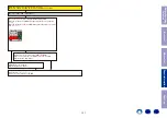
When the results of check item (3-16.11.) are "

00

"

(Detection of HPD is not OK / Detection of RXSENSE is not OK )

Check item(3-16.17.).

 Checking the HPD and RXSENSE. : 

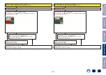
Does the test point of RXSENSE close to the HDMI output terminal 

[

N3401

] indicate the (3.3V)?

Does the voltage of HPD test point close to the HDMI output terminal 

[

N3401

] indicate "Hi" (3-5 V)?

N3401

HDMI OUT

[MONITOR2]

D2+ D2- D1+ D1- D0+ D0- CK+ CK-

HPD

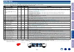
Checking the HPD/RXSENSE status register.  (OUT2)

HDMI Tx [

U3401

] is faulty.

Replace with a new device.

Recheck from 

check item (3.4.)

If it does not work, replace the PCB.

Check for a short circuit in the TMDS/ HPD line.

If there is no problem, the HDMI Tx [

U3401

] is faulty.

Replace with a new device.

NO

YES

Before Servicing 

This Unit

Electrical

Mechanical

Repair Information

Updating

135

Summary of Contents for AVC-X6300H

Page 1: ...anuals denon com AVCX6500H EU EN index php AP http manuals denon com AVCX6500H AP ZH index php JP http manuals denon com AVCX6500H JP JA index php Upload is planned for the time of a future press rele...

Page 2: ...ONLINE PARTS LIST Accessing the Parts List Searching Part Numbers or Ref Numbers NOTE FOR PARTS LIST SERIAL NUMBER Serial Number Organization SKU Code of this Unit POST SERVICE PRECAUTIONS Initializi...

Page 3: ...c diagrams and parts lists be sure to use the designated parts Be sure to mount parts and arrange the wires as they were originally placed For safety seasons some parts use tapes tubes or other insula...

Page 4: ...PUT CONDITION 4 CIRCUIT AND PARTS ARE SUBJECT TO CHANGE WITHOUT PRIOR NOTICE Electrostatic breakdown of the semi conductors or optical pickup may occur due to a potential differ ence caused by electro...

Page 5: ...bers or Ref numbers 1 Enter the part number or Ref number in the search window of the Parts List and press the search button 2 The search results are displayed The name of the sheet in which the searc...

Page 6: ...Organization The 14 digit serial number that contains the code of the manufacturing plant and the manufacturing date SKU code 14 digits Factory code Cumulative serial number Manufactured Year month T...

Page 7: ...etwork related settings NOTE If the unit fails to enter the service mode in step 3 repeat the procedure from step 1 Initializing the device restores the customized settings to the factory settings Wri...

Page 8: ...SCH27_MAIN DAC SCH28_FRONT HDMI USB SCH29_SMPS SCH30_232C PHONO SCH31_P AMP1 SCH32_P AMP2 SCH33_SPEAKER SCH34_REG SCH35_FLD PRINTED CIRCUIT BOARDS DIGITAL AUDIO VIDEO FRONT HDMI FRONT USB CONNECT 1 CO...

Page 9: ...C 5 FB 4 NC 3 LX 1 2 3 4 5 6 7 D 6 G 2 S 1 D 3 G 5 S 4 1 2 3 3 4 5 6 11 10 9 8 13 12 1 2 GND 7 VCC 14 MDAX_LED ILLUMI_LED DIRECT_LED DOORDET FL_CE2 RCOUT KILLIR FLASHERIN FL_CTRL VAUXV H PR H PL VAUXR...

Page 10: ...Q12 90 VCC 91 PC0 IRQ14 92 VSS 93 P73 94 PB7 TXD9 95 PB6 RXD9 96 PB5 SCK9 97 PB4 98 PB3 SCK4 SCK6 99 PB2 100 PB1 TXD4 TXD6 IRQ4 DS 101 P72 102 P71 103 VCC 104 PB0 RXD4 RXD6 IRQ12 105 VSS 106 PA7 107 P...

Page 11: ...2 Q7 13 Q6 14 Q5 15 OE 16 VDD 1 STB 2 DATA 3 CLK 4 Q1 5 Q2 6 Q3 7 Q4 8 VSS 9 QS 10 Q S 11 Q8 12 Q7 13 Q6 14 Q5 15 OE 16 VDD 1 STB 2 DATA 3 CLK 4 Q1 5 Q2 6 Q3 7 Q4 8 VSS 9 QS 10 Q S 11 Q8 12 Q7 13 Q6 1...

Page 12: ...ARC64fs ARCI2S2 ARC256fs ARCI2S0 ARCI2S1 ARC_MUTE ARCSPDIF ARCI2S3 100x4 R1206 KRC402E RTK Q8011 KRC402E RTK Q8012 KRC402E RTK Q8013 KRC402E RTK Q8014 10K R9231 10K R9232 P4 ARC64fs DSDSCK N2 ARCSPDI...

Page 13: ...NDIRERR MAINDIR256fs MAINDIR64fs MAINDIRfs Z2NETADC_fs Z2NETADC_64fs Z2NETADC_256fs Z2NETADC_DATA Z2NETADC_R Z2NETADC_L COAX2 OPT1 COAX1 OPT2 Z3DAC_DEMP Z2DAC_DEMP 7 8 5 6 7 8 5 6 1 2 3 4 1 SCL 2 SDA...

Page 14: ...2 107 VDD_INT 108 AMI_ACK 109 GND 110 THD_M 111 THD_P 112 VDD_THD 113 VDD_INT 114 VDD_INT 115 MS1 116 VDD_INT 117 WDT_CLKO 118 WDT_CLKIN 119 VDD_EXT 120 ADDR23 121 ADDR22 122 ADDR21 123 VDD_INT 124 AD...

Page 15: ...09 GND 110 THD_M 111 THD_P 112 VDD_THD 113 VDD_INT 114 VDD_INT 115 MS1 116 VDD_INT 117 WDT_CLKO 118 WDT_CLKIN 119 VDD_EXT 120 ADDR23 121 ADDR22 122 ADDR21 123 VDD_INT 124 ADDR20 125 ADDR19 126 VDD_EXT...

Page 16: ...108 AMI_ACK 109 GND 110 THD_M 111 THD_P 112 VDD_THD 113 VDD_INT 114 VDD_INT 115 MS1 116 VDD_INT 117 WDT_CLKO 118 WDT_CLKIN 119 VDD_EXT 120 ADDR23 121 ADDR22 122 ADDR21 123 VDD_INT 124 ADDR20 125 ADDR1...

Page 17: ...SDA10 28 VDD_EXT 29 VDD_INT 30 ADDR11 31 ADDR12 32 ADDR17 33 ADDR13 34 VDD_INT 35 ADDR18 36 RESETOUT RUNRSTIN 37 VDD_INT 38 DPI_P01 39 DPI_P02 40 DPI_P03 41 VDD_INT 42 DPI_P05 43 DPI_P04 44 DPI_P06 45...

Page 18: ...L3622 C3674 1200P C3659 10 6 3 0 R3628 6 2K R3643 1000P C3682 R3621 15K 6 2K R3641 0 1 C3650 0 1 C3768 BLM21PG221 L3608 C3629 10 6 3 1000P C3769 C3608 1u R3600 47K C3665 1u 10 6 3 C3612 10 R3656 R3642...

Page 19: ...2046 33 R2049 33 R2048 10K R2028 10K R2027 C2037 1000P C2016 0 1 22 6 3 C2006 C2011 4 7u C2022 0 1 C2031 1000P OPEN R2029 7810_LLC 7810_DO8 7810_D10 7810_DO9 7810_D14 7810_D12 7810_D11 7810_D13 7810_D...

Page 20: ...18 5V 19 HP_DET 1 TX2 2 TX2_SHLD 3 TX2 4 TX1 5 TX1_SHLD 6 TX1 7 TX0 8 TX0_SHLD 9 TX0 10 TXC 11 TXC_SHLD 12 TXC 13 CE_REMOTE 14 N C 15 DDC_SCK 16 DDC_SDA 17 GND 18 5V 19 HP_DET 1 TX2 2 TX2_SHLD 3 TX2...

Page 21: ...LD 6 TX1 7 TX0 8 TX0_SHLD 9 TX0 10 TXC 11 TXC_SHLD 12 TXC 13 CE_REMOTE 14 N C 15 DDC_SCK 16 DDC_SDA 17 GND 18 5V 19 HP_DET 1 TX2 2 TX2_SHLD 3 TX2 4 TX1 5 TX1_SHLD 6 TX1 7 TX0 8 TX0_SHLD 9 TX0 10 TXC 1...

Page 22: ...SPICS IP_MITXO IP_MOTXI IP_SPISCK TX256fs DSDMCK TX_ARC1OUT TX_ARC2OUT TXI2S0 DSD1 TXfs DSD5 4 7Kx4 R2898 4 7Kx4 R2899 4 7Kx4 R2899 4 7Kx4 R2899 4 7Kx4 R2898 4 7Kx4 R2899 R2900 4 7K A7 TX_ARC2OUT B7 T...

Page 23: ...X_DDRVREF TX_DDRVREF C3025 10 6 3 C3010 0 1 C3011 0 1 C3014 0 1 C3013 0 1 C3016 0 1 C3012 0 1 C3015 0 1 C3041 0 1 C3035 0 1 C3039 0 1 C3036 0 1 C3037 0 1 C3040 0 1 C3038 0 1 C3049 1000P C3024 1000P R3...

Page 24: ...4 R3203 47 R3214 22 R3224 DGND DV3 3V VPLD_TRANS0 L14 VPLD_TRANS2 N12 VPLD_TRANS1 L13 SUB_TDO SUB_TMS VP_TDI L6 VP_TCK P3 VP_TMS N4 VP_TDO M5 TDO1_TDI2 SUB_TCK 10x4 R3218 10x4 R3218 10x4 R3218 10x4 R3...

Page 25: ...25 P1TX0P 26 AVDD33TX 27 P1TX0M 28 P1TXCP 29 AVDD11TX 30 P1TXCM 31 VSS 32 VDD11 33 P0TX2P 34 AVDD11TX 35 P0TX2M 36 P0TX1P 37 AVDD11TX 38 P0TX1M 39 P0TX0P 40 AVDD33TX 41 P0TX0M 42 P0TXCP 43 AVDD11TX 44...

Page 26: ...4fs ARCI2S0 ARCSPDIF ARCI2S3 DGND CEC3 3V R3802 OPEN C3817 1000P R3804 OPEN 10K R3803 C3814 0 1 C3815 0 1 C3807 1u C3808 1u HPDout R3801 2 2K UDZS3 6B D3802 R3818 4 7K R3817 4 7K 33x4 R3900 33x4 R3900...

Page 27: ...CS_WR PLD_TMS_WR DSP_SF_SI_WR DSP_SF_CK_WR DSP_SF_SI_WR PLD_TDI_WR DSP_SF_CK_WR DSP4_SF_SO_WR DSP_SF_CK_WR DSP3_SF_SO_WR DSP_SF_CS_WR DSP_SF_CS_WR DSP2_SF_SO_WR DSP_SF_SI_WR DSP_SF_SI_WR NET_TDM_DOUT...

Page 28: ...28 29 30 31 32 33 1 2 3 VIN 1 ON OFF 2 GND 5 NC 4 VOUT 3 8 GPIO2 INT 7 RST 6 SEN 5 SDIO 4 SCLK 3 VCC 2 ROUT 1 LOUT 12 CG 11 CG 10 CG 9 CG 1 STB 2 DATA 3 CLK 4 Q1 5 Q2 6 Q3 7 Q4 8 VSS 9 QS 10 Q S 11 Q...

Page 29: ...9 NC 28 OutA1 27 OutB1 26 REF_A 25 OutA2 24 OutB2 23 REF_B 22 OutA3 21 OutB3 20 NC 19 NC 18 CLOCK 17 DATA 2 InA1 3 InB1 4 InA2 5 InB2 6 InA3 7 InB3 8 InA4 9 InB4 10 InA5 11 InB5 12 InA6 13 InB6 14 InA...

Page 30: ...0P R3568 220 C3553 470P 10 63 C3531 R3551 100K R3552 100K R3569 220 R3521 100K R3520 100K 10 63 C3530 R3566 220 C3551 470P R3518 100K 10 63 C3529 R3565 220 R3567 220 10 63 C3527 R3549 100K R3548 100K...

Page 31: ...75 R3702 75 R3708 OPEN R3704 75 C3711 OPEN C3710 10 6 3 R3709 OPEN C3706 10 6 3 OPEN K3504 OPEN K3502 6P RCA 637G K3503 6P RCA 637G K3503 R3729 75 R3761 75 R3753 75 R3732 0 R3724 0 R3723 0 75 R3713 10...

Page 32: ...29 30 31 32 33 DA3 3V M3 3V AEXP_STB AEXP_DATA AEXP_OE TUGPIO AEXP_CLK TEDET FANDET_ON FANDET_HIGH DCDET ASODET TURST TUSEN TUSDA TUSCL THERMALF THERMALE CURRENTDET AMPSIGDET PREGND PREGND PREGND 7V...

Page 33: ...6 5 4 3 2 1 13 12 11 10 9 8 7 6 5 4 3 2 1 13 12 11 10 9 8 7 6 5 4 3 2 1 13 12 11 10 9 8 7 6 5 4 3 2 1 13 12 11 10 9 8 7 6 5 4 3 2 1 13 12 11 10 9 8 7 6 5 4 3 2 1 13 12 11 10 9 8 7 6 5 4 3 2 1 13 12 1...

Page 34: ...C5066 0 1 C5071 C5068 1000P PCM5100PWR U5006 2 2u C5072 10K R5053 100 10 C5069 2 2u C5073 R5051 470 C5076 2200P 0 1 C5067 R5046 10K C5078 OPEN C5070 4 7u 47K R5048 C5075 2200P R5047 10K R5045 10K NETR...

Page 35: ...42 0 C7516 0 C7523 0 C7554 0 C7530 0 C7552 0 C7517 0 C7528 0 C7548 0 C7518 0 C7538 0 C7519 0 C7515 0 C7551 0 C7555 0 C7545 0 C7529 0 C7520 0 C7541 0 C7532 0 C7531 DA3 3V To_8U 210242 6 N9029 CONNECT 1...

Page 36: ...22 R5514 22 To_8U 310232 N8001 DIGITAL_UNIT 19 19 44431053810AS_S HDMI_CABLE_HOLDER A Z9999 TCA9517DGKR U5501 C5502 0 1 R5513 10K R5506 1 8K R5505 1 8K FRONT_HDMI_UNIT 8U 210242 5 FRON_HDMI_BRACKET Z5...

Page 37: ...PEN C6521 OPEN R6523 3 3K U6501 PC123X2YFZ1B 0 R6532 1K R6533 Z6516 3X10_CBTS S Z KIA2431AS D6524 KTC3875S Q6502 44431034100AS Z6505 CLIP TRK 24 1 5K R6520 10K R6519 UNFIX110157Z1 HEAT_SINK SMPS A Z65...

Page 38: ...933 75 R3936 OPEN OPEN D3911 R3934 75 OPEN D3912 OPEN D3913 OPEN C6534 OPEN C6535 OPEN R3914 OPEN R3915 OPEN Q3907 OPEN Q3908 OPEN R3955 OPEN R3954 OPEN R3953 OPEN R3958 OPEN R3957 OPEN R3956 OPEN C39...

Page 39: ...H R134 10 C116 0 047 R135 10 SHORT J106 1 100 C114 1 100 C122 1 100 C115 1 100 C121 C104 100P HN4A06J Q101 Q105 2N5401S Q113 2N5551S R136 470 R137 220 Z107 OPEN Z106 OPEN 5P EHs N102 To_8U 210242 3 L_...

Page 40: ...6QB301T V201 C211 0 1 R218 47 R206 470 R202 1 5K R225 0 47 R230 5 6K R207 470 R215 OPEN 220P C209 R227 10K DHCT A3 Q209 SHORT J207 KDS160 D201 R220 330K 2200P C203 SHORT J208 PRF18BC471QB5RB Z201 D205...

Page 41: ...0P C6042 SURROUND_BACK R HEIGHT2 L SURROUND_BACK L FRONT R SURROUND L CENTER FRONT L MST 1030V2 02 K6011 HEIGHT1 L MST 1030V2 02 K6010 HEIGHT2 R MST 1030V2 02 K6008 HEIGHT1 R MST 1030V2 02 K6009 SURRO...

Page 42: ...1 4 PRE GND OPEN R6489 OPEN R6485 OPEN R6484 OPEN R6486 DAGND Z6205 3X8_CBS B 44741010704AS RADIATOR Z6416 OPEN C6619 B6901 OPEN B6902 OPEN OPEN N5811 OPEN C5811 OPEN Z5812 OPEN C5814 OPEN B5811 OPEN...

Page 43: ...220 S6405 TACT R6441 330 R6442 330 S6412 TACT S6415 TACT R6427 82 S6419 TACT R6424 100 S6408 TACT R6422 82 S6404 TACT R6438 220 S6407 TACT S6403 TACT R6434 270 S6420 TACT S6413 TACT R6447 330 R6436 22...

Page 44: ...162 39 2 1 40 1 TOP 19 TOP 1 10 1 TOP 7 11 1 TOP 1 TOP 7 10 TOP 1 1 TOP 7 1 7 TOP TOP 1 10 1 TOP 7 1 176 133 132 89 88 45 44 10 TOP 1 7 TOP 1 A 1 16 T 109 108 73 72 36 1 144 37 63301023210AS 8U 310232...

Page 45: ...R3723 R3724 R3530 R3531 R3532 R3533 R3534 R3535 R3729 R3536 R3537 R3538 R3345 R3539 R8166 R3346 R8167 R3347 R8168 R3348 L3614 R8169 R3349 L3615 R3731 R3732 R3734 R3735 R3736 R3737 R8170 R3350 R3738 R8...

Page 46: ...7543 C7544 C5029 C7545 R5001 C7546 R5002 R5003 C7547 R5004 C7548 R5005 R5006 R5007 R5008 R5009 C5032 C5033 C5034 R5201 C5035 C7551 C5036 R5202 C7552 C5037 R5203 C7553 R5204 R5010 C5038 C7554 C7555 C50...

Page 47: ...204 20 0 JV20 J6010 22 5 B6901 J6011 17 5 B6902 J6206 20 0 J6012 17 5 B6903 J6207 20 0 J6013 25 0 J6208 20 0 J6209 20 0 15 0 JV25 15 0 J6015 JV28 JV29 J6210 20 0 J6211 20 0 J6212 20 0 17 5 JV31 JV33 7...

Page 48: ...R202 R203 R208 R209 C206 C210 1 1 1 Q201 R215 R216 R217 R220 R221 R226 R227 R228 R229 R230 R231 R232 R233 C204 C207 C208 C211 C212 C213 C217 C218 C219 C220 C223 D201 D202 D205 D210 Z201 Q202 Q203 Q20...

Page 49: ...tware Digital input Voltage due to hardware of analog input OFFSET of SW NONE 9 5dB 12 5dB 35dBFS A D IN 20dBFS DIG IN LINE H POUT TO ZONE3 SPEAKER OUT DSP x4pcs NJU72343 GAIN ADJ PRE OUT MUTE TO ZONE...

Page 50: ...L 2 0dB 0 5dB 2 5dB SW YES DIGITAL 2 0dB 0 5dB 3 0dB 0 5dB Basic OFFSET of VOL 0dB indication valude Fine tuning by software Digital input OFFSET of SW NONE OFFSET of A D input 20dBFS DIG IN SPEAKER O...

Page 51: ...g by software Digital input Voltage due to hardware of analog input Correction of Subwoofer OFFSET of A D input DSP x4pcs NJU72343 GAIN ADJ PRE OUT MUTE AK4458 D A PLD PRE OUT 11 5dB L P F GAIN 6 5dB...

Page 52: ...YES DIGITAL 2 0dB 0 5dB 2 5dB SW YES DIGITAL 2 0dB 0 5dB 3 0dB 0 5dB Basic OFFSET of VOL 0dB indication valude Fine tuning by software Digital input OFFSET of SW NONE OFFSET of A D input 20dBFS DIG IN...

Page 53: ...SIGNAL LEVEL 20dBFS DIG IN SPEAKER OUT 2 0Vrms 0dBFS 10dBFS 20dBFS 30dBFS 40dBFS PCM5100 2 5dB PRE OUT 150mVrms Z3 PRE OUT MUTE MONO HPF MONO MONO HPF MONO NJW1194V Z2 PRE OUT MUTE NJW1194V MAX OUTPUT...

Page 54: ...HL2 HL1 HR1 HR2 HR1 HL1 FR SL FL C SR SL FR C FL SR Z2R Z2L Z2L Z2R Z2L Z2R SBR SBL HR1 HL1 HR1 HL1 Z3L Z3R Z3L Z3R Z3L Z3R Z3L Z3R Z2R Z2L SBR SBL HR1 HL1 HL1 HR1 FL FR SR C SBL SL SBR FL FR SR C SB...

Page 55: ...ET I2S_NET CLK DLHD Z2_SPDIF Z3_SPDIF CLK Z2NET_I2S Z2NET_I2S PLLOUT SPDIF_Z2HDMI REFCLK Z2NETDAC_MCLK I2S_eARC DSD_eARC SPDIF_HDMIRX SPDIF_HDMIRX I2S DSD_eARC SPDIF_eARC SPDIF_eARC SPDIF_Z2HDMI SPDIF...

Page 56: ...HDMI INPUT HDMI 6 HDMI 1 MONITOR1 HDMI 3 VIDEO DECODER ADV7180 Blu ray to DIGITAL AUDIO TMDS FROM D AUDIO I2S TMDS INPUT TMDS I P scaler GUI ADV8003 TMDS HDMI 5 TMDS DVD DDR2 TMDS ZONE1 INPUT TMDS IN...

Page 57: ...L212 DA1 1V 1 1 1V D5V 5 2V form_MAIN DA1 1V 1 NET5V IN OUT DC_DC_CONV CEC_POWER XCL212 CEC3 3V 3 3V D5V 5 2V form_MAIN CEC1 1V1 FLD_AC IN OUT DC_DC_CONV POWER XCL212 M3 3V 3 3V D5V 5 2V CEC5V CEC1 1V...

Page 58: ...NC open 21 RES RESET I Reset signal input pin 22 XTAL P37 XTAL I Pins for a crystal resonator Xin 12MHz 10 23 VSS VSS Ground pin 24 EXTAL P36 EXTAL Pins for a crystal resonator Xin 12MHz 10 25 VCC VCC...

Page 59: ...STBY Function 103 VCC VCC Power supply pin 104 PB0 RXD4 RXD6 IRQ12 Z3PLD_ERR I L L L Detect PLD error from Audio PLD 105 VSS VSS Ground pin 106 PA7 ISEL_A I I I I Input selector Rotary encoder signal...

Page 60: ...up A 1 7 MPIO_C0 I O Yes Multipurpose I O Group C 1 8 MPIO_C1 I O Yes Multipurpose I O Group C 1 9 MPIO_C2 I O Yes Multipurpose I O Group C 1 10 MPIO_C3 I O Yes Multipurpose I O Group C 1 11 MPIO_B0 I...

Page 61: ...nboard pull down resistor 50 k typical 5 CMOS Schmitt trigger input PCM9211 BLOCK DIAGRAM Clock Data Recovery MPIO_A SELECTOR MPIO_C SELECTOR MPIO _B SELECTOR ADC Com Supply MPO0 1 SELECTOR MPO 0 MPO...

Page 62: ...1 165 VDD_INT 34 VDD_INT 78 ADDR21 122 DATA12 166 ADDR18 35 NC 79 VDD_INT 123 DATA14 167 RESETOUT RUNRSTIN 36 NC 80 ADDR20 124 DATA13 168 VDD_INT 37 NC 81 ADDR19 125 VDD_INT 169 DPI_P01 38 NC 82 VDD_E...

Page 63: ...H 32 bit I2S 16 PS I I2C pin H Control Mode Select Pin L I2C Bus serial control mode H Parallel control mode Hi Z CAD0_SPI I I2C pin L Chip Address 0 Pin in 3 wire serial control mode 17 I2C I Contro...

Page 64: ...3 AOUTL3P AOUTL3N AOUTR3P 8X Interpolator SCF SCF AOUTR4N VREFH4 VREFL4 AOUTL4P AOUTL4N AOUTR4P Vref 8X Interpolator SCF SCF Vref SDTI3 DSDR2 TDMO1 SDTI4 DSDL3 TDMO2 DSDR3 DSDL4 DSDR4 VDD18 LDO DZF SM...

Page 65: ...ces Part Number Dynamic Range SNR THD PCM5102 112dB 112dB 93dB PCM5101 106dB 106dB 92dB PCM5100 100dB 100dB 90dB spacer Figure 1 PCM510x Functional Block Diagram NJU72343 AUDIO VIDEO U3215 U3216 No Sy...

Page 66: ...Bch input2 23 OutA3 Ach output3 8 NC 24 REF_B Bch reference potential 9 NC 25 REF_A Ach reference potential 10 InA3 Ach input3 26 OutB2 Bch output2 11 InB3 Bch input3 27 OutA2 Ach output2 12 NC 28 NC...

Page 67: ...k 15 DA Serial Data Input 16 TSA B Test pin 17 Solder composition is Sn 3Ag 0 5Cu 18 Field of vision is a minimum of 21 8 from the lower side q Y2 1G B A 2G B A 3G B A 4G B A 5G B A 6G B A 7G B A 8G B...

Page 68: ...0046 SP A FRONT RCSHP0230062 RCSHP0230047 SP B FRONT RCSHP0230063 FORMAT SHARP DATA CONSTRUCTION 15bits C14 0 C15 0 NOT INVERTED 1 INVERTED REMOTE ID 1 SYSTEM ADDRESS C1 C5 EXTENSION BIT C12 C13 No Da...

Page 69: ...No Data C6 C11 Key Name RCSHP0210000 RCSHP0210016 RCSHP0210001 RCSHP0210017 RCSHP0210002 RCSHP0210018 ZONE3 TV AUDIO RCSHP0210003 RCSHP0210019 ZONE3 CBL SAT RCSHP0210004 RCSHP0210020 ZONE3 GAME RCSHP0...

Page 70: ...10012 0 0 1 1 0 0 0 0 0 0 TRIGGER 1 ON RCKSK0410013 1 0 1 1 0 0 0 0 0 0 TRIGGER 1 OFF RCKSK0410014 0 1 1 1 0 0 0 0 0 0 TRIGGER 2 ON RCKSK0410015 1 1 1 1 0 0 0 0 0 0 TRIGGER 2 OFF RCKSK0410016 0 0 0 0...

Page 71: ...0 0 0 1 0 1 FHL LEVEL DOWN RCKSK0410651 1 1 0 1 0 0 0 1 0 1 FHR LEVEL UP RCKSK0410652 0 0 1 1 0 0 0 1 0 1 FHR LEVEL DOWN RCKSK0410656 0 0 0 0 1 0 0 1 0 1 Front Display Dimmer RCKSK0410669 1 0 1 1 1 0...

Page 72: ...K0430031 1 1 1 1 1 0 0 0 0 0 ZONE2 ENTER RCKSK0430034 0 1 0 0 0 1 0 0 0 0 ZONE2 RETURN RCKSK0430036 0 0 1 0 0 1 0 0 0 0 ZONE2 MEMORY RCKSK0430292 0 0 1 0 0 1 0 0 1 0 ZONE2 QUICK SELECT 1 RCKSK0430293...

Page 73: ...9 1 0 0 0 1 1 1 0 1 0 ZONE3 VOLUME DOWN RCKSK0450370 0 1 0 0 1 1 1 0 1 0 ZONE3 VOLUME MUTE RCKSK0450370 1 1 0 0 1 1 1 0 1 0 ZONE3 VR MUTE RCKSK0450372 0 0 1 0 1 1 1 0 1 0 ZONE3 VR PRESET1 0dB RCKSK045...

Page 74: ...CKSK0410179 1 1 0 0 1 1 0 1 0 0 PRESET 4 Numeric 4 RCKSK0410180 0 0 1 0 1 1 0 1 0 0 PRESET 5 Numeric 5 RCKSK0410181 1 0 1 0 1 1 0 1 0 0 PRESET 6 Numeric 6 RCKSK0410182 0 1 1 0 1 1 0 1 0 0 PRESET 7 Num...

Page 75: ...MECHANICAL DISASSEMBLY Flowchart 1 FRONT PANEL ASSY 2 RADIATOR ASSY 3 DIGITAL PCB 4 TRANS EXPLODED VIEW PACKAGING VIEW Before Servicing This Unit Electrical Mechanical Repair Information Updating 75...

Page 76: ...nd EXPLODED VIEW POWER TRANS Ref No of EXPLODED VIEW M 08 RADIATOR ASSY DISASSEMBLY 2 RADIATOR ASSY and EXPLODED VIEW L AMP CONNECT PCB Ref No of EXPLODED VIEW B 02 3 R AMP CONNECT PCB Ref No of EXPLO...

Page 77: ...VR X6500H E3 are used in this manual The viewpoint of each photograph Shooting direction X View from the top Shooting direction C Shooting direction D Shooting direction A Shooting direction B Proceed...

Page 78: ...C BLUE FR RED SR BROWN SBR GRAY H1R YELLOW H2R PURPLE L AMP CONNECT R AMP CONNECT STYLE PIN Proceeding TOP COVER DIGITAL PCB 1 Remove the screws 2 Remove the STYLE PINs and connectors Remove the FFC...

Page 79: ...P COVER RADIATOR ASSY or BACK PANEL ASSY TRANS 1 Remove the screws Remove the connector 4 TRANS N6201 N6012 x4 N6401 N6501 STYLE PIN Before Servicing This Unit Electrical Mechanical Repair Information...

Page 80: ...B04 9 B04 10 B01 B02 1 B02 2 B02 3 B02 4 B02 5 B02 6 B02 7 B02 8 B02 9 B03 1 B03 6 B03 7 B03 8 B03 9 B03 10 B03 11 B03 12 B03 13 B03 14 z z z S15 S15 Precautions when a xing the BADGE 1 The BADGE is...

Page 81: ...ttp dmedia dmglobal com Document DocumentDetails 24838 P7 P8 P9 P26 P24 P23 P10 P11 P39 P27 P30 P25 P33 P34 P28 P29 P31 P12 P13 P14 P15 P16 P17 P18 P19 P20 P21 P22 P32 P06 P04 P03 P03 P36 P35 P38 P05...

Page 82: ...AL BLOCK SPECIAL MODE Special mode setting button 1 Version Display Mode 2 PANEL REMOTE LOCK Selection Mode 3 1 Selecting the Mode for Service related 3 2 Protection History Display Mode 3 3 232C Stan...

Page 83: ...here any parts not fully connected into the connectors that connect the PCBs Is DC5V output even when the connector N6001 supplying power from the SMPS PCB to the DIGITAL PCB is removed Check the circ...

Page 84: ...3328 C3710 C3711 R3301 C3712 R3302 C3713 R3303 C3714 R3304 R3305 C3715 R3306 C3716 R3307 C3717 R3308 C3718 R3309 Q3521 C3719 Q3523 R3501 R3502 R3503 R3310 R3504 C3720 R3311 R3505 R3312 R3506 R3313 R35...

Page 85: ...onitor out R3742 Q2 Component Cb to Monitor out R3746 Q3 Component Cr to Monitor out R3750 Q4 Component Y to DIGITAL PCB R3744 Q5 Component Cb to DIGITAL PCB R3748 Q6 Component Cr to DIGITAL PCB R3752...

Page 86: ...HDMI DVI cable Use a certified HDMI cable with the HDMI mark Replace the HDMI DVI cable with the one shorter than 5m 2m is recommended and check again Use an High speed HDMI cable with Ether net or Hi...

Page 87: ...ERR displayed Check the unit The TV is faulty Check the circuits around the IP SCALER U2800 DIGITAL PCB and DDR2 U3000 U3001 If there appear to be no problems U2800 or U3000 U3001 is faulty See HDMI...

Page 88: ...4 INPUT SURROUND MODE SOURCE Audio output OK HDMI Legacy PCM2ch or DolbyDigital or dts CHECK 6 INPUT Connect AVR s connected in HDMI audio out put OK HDMI This unit s HDMI OUT Other AVR s HDMI IN Sett...

Page 89: ...the emitter resistor Replace the base resistor Replace the trimmer potentiometers NO NO NO NO NO NO YES Check the CPU 4 3 Analog audio No audio output Are the N9028 5 7pins in the A AUDIO VIDEO PCB re...

Page 90: ...LAN cable correctly inserted Insert the LAN cable correctly and then turn on the power again Check the connection environment Checking the unit YES YES YES Can the output voltage 5V to Q8007 FET SW b...

Page 91: ...y Is the antenna cable inserted correctly into Net work Module Is the Bluetooth device compatible with the A2DP profile Is the Bluetooth function enabled on the Blue tooth device Connect the antenna c...

Page 92: ...is faulty Connect the connectors correctly 5 3 Cannot recognize the connected USB device YES NO NO NO Checking the unit If no picture is output YES Check the VIDEO circuit Are digital video signals NE...

Page 93: ...D3414 R3411 D3415 C2881 D3416 R3606 R3413 D3417 C2883 R3414 D3418 R8040 R209 D3419 R2669 R8041 D3801 R3415 R 2 4 7 6 R8042 R3416 C3633 R2477 R8043 R3223 R3417 1 U2800 U3000 U3001 N6001 Q8009 N8001 U3...

Page 94: ...7u C6543 4 7u C6544 4 7u C6545 4 7u C6528 22 R6513 44741010600AS HEATSINK Z6503 R6534 OPEN R6538 0 R6535 OPEN C6504 OPEN C6507 OPEN C6508 OPEN 1SR154 D6526 D6527 1N4003 D 1 G 2 S 3 3 1 2 1 2 3 4 4 10...

Page 95: ...P61 140 VSS 141 P60 142 VCC 143 PD7 IRQ7 AN107 144 PG1 145 PD6 IRQ6 AN106 146 PG0 147 PD5 IRQ5 AN113 148 PD4 IRQ4 AN112 149 P97 150 PD3 IRQ3 AN111 151 VSS 152 P96 153 VCC 154 PD2 IRQ2 AN110 155 P95 15...

Page 96: ...ME INPUT SELECTOR I2S SELECTOR I2S AK4458 x 2 PLD PCM9211PTR DIR INPUT ANALOG 2CH INPUT NETWORK INPUT DIGITAL INPUT HDMI INPUT HDMI FRONT ETHERNET Wifi USB OPTICAL COAXIAL A D_INPUT D A_OUTPUT ADC BLO...

Page 97: ...for deformed pins OK NG Check by following the flow chart for 3 Starting detecting the point of failure NOTE After checking troubleshooting 3 HDMI DVI check 3 Starting detecting the point of failure R...

Page 98: ...2 b Figure 1 Device Connection Method 2 Preparations for checking HDMI Switcher reception transmission register 2 3 Device configuration method PC settings Execute the serial communication program Te...

Page 99: ...exiting Setup Assistant execute the above Display changes Figure 4 Change of the Display of the Communication Start Button Name Press Figure 6 AVR settings All the indicatorLights Figure 6 FLD Displa...

Page 100: ...DMI SW2 U2601 MN864788 H1 05 Check item 3 7 1 Communication Error with VIDEO DECODER U2001 ADV7180 H1 06 Check item 3 4 1 Communication Error with GUI IC U2800 ADV8003 H1 08 Check item 3 8 1 Communica...

Page 101: ...e player played back on the TV correctly in each case ZONE2 OUT HDMI IN 1 4 Check item 3 4 Does a video signal come from HDMI OUT to TV correctly Turn Video Conversion OFF on the setup menu SETUP MENU...

Page 102: ...place the PCB Recheck from check item 3 1 If it does not work replace the PCB Checking device U3401 MN864787 3 1 Error Code H1 01 failure detection procedure NO YES NO YES Go to next page YES Checking...

Page 103: ...cation line Check HDMI SW U2601 or U2401 HDMI Tx U3401 and CPU U6201 patterns as well as soldering If there is no problem go to the next step Check the HDMI SW1 Remove the damping resistor R2460 R2461...

Page 104: ...resistor If there is still a problem the HDMI SW1 U2401 is faulty Replace with a new device The power supply circuit is faulty Replace the PCB Recheck from check item 3 1 If it does not work replace...

Page 105: ...3 Error Code H1 03 failure detection procedure NO YES NO YES Checking the reset waveform HDMI SW2 Check item 3 3 3 Checking the reset waveform Check the waveform Is the waveform of the TP near the HDM...

Page 106: ...06 failure detection procedure NO GUI U2800 is faulty Replace with a new device Recheck from check item 3 1 If it does not work replace the PCB The power supply circuit is faulty Replace the PCB NO Y...

Page 107: ...the I2C communication line again after replacing the FET Q2001 If there is still a problem the GUI U2800 is faulty Replace with a new device Check the I2C communication line GUI U2800 is faulty Repla...

Page 108: ...is defective Replace their IC Or replace the substrate 3 6 Error Code H1 15 failure detection procedure Checking device U2801 W25Q128JVFIQ Check item 3 6 1 Write to the GUI ROM Recheck from check ite...

Page 109: ...een CPU U6201 and VIDEO DECODER U2001 If there is no problem the VIDEO DECODER U2001 is faulty Replace with a new device Recheck from check item 3 7 1 If it does not work replace the PCB NO Examples o...

Page 110: ...ror Code H1 08 failure detection procedure NO DSP U101 is faulty Replace with a new device Recheck from check item 3 1 If it does not work replace the PCB The power supply circuit is faulty Replace th...

Page 111: ...well as soldering If there is no problem go to the next step Check the SPI communication line DSP1 DSP U101 is faulty Replace with a new device YES The diagram shows an example Signal patterns vary de...

Page 112: ...ce U201 ADSP21487 Go to next page NO DSP U201 is faulty Replace with a new device Recheck from check item 3 1 If it does not work replace the PCB The power supply circuit is faulty Replace the PCB NO...

Page 113: ...as soldering If there is no problem go to the next step Check the SPI communication line DSP2 DSP U201 is faulty Replace with a new device YES The diagram shows an example Signal patterns vary dependi...

Page 114: ...v Check item 3 10 2 Check the SPI communication line Check the CPU Is the SPI waveform of the TP near the DSP U301 correct like the one shown in the diagram when the power is turned on U301 CS Check i...

Page 115: ...v Check item 3 11 2 Check the SPI communication line Check the CPU Is the SPI waveform of the TP near the DSP U401 correct like the one shown in the diagram when the power is turned on U401 CS Check i...

Page 116: ...he communication line Check the CPU Is the waveform of the TP near the DIR U7004 correct like the one shown in the diagram when the power is turned on U7004 25pin CLK 24pin MOSI 26pin CS 23pin MISO Ch...

Page 117: ...ply circuit is faulty Replace the PCB Recheck from check item 3 1 If it does not work replace the PCB Checking device U3802 SiI9437 NO YES NO YES YES Checking the reset waveform ARC IC Check item 3 13...

Page 118: ...s the return value C4 or C0 IN6 A2 or A0 IN7 91 or 90 Example i 002E 00FF 0001 C4 00 or 04 Detection of DDC is not OK 22 or 11 Detection of DDC is OK Go to check item 3 14 4 Go to check item 3 14 3 Go...

Page 119: ...Replace with a new device Recheck from check item 3 2 If it does not work replace the PCB HDMI Switcher1 U2401 is faulty Replace with a new device Check for a short circuit in the 5V line and the 5V...

Page 120: ...U2401 from the HDMI input terminal If there is no problem the HDMI Switcher1 U2401 is faulty Replace with a new device HDMI Switcher1 U2401 is faulty Replace with a new device Recheck from check item...

Page 121: ...3 14 9 Checking the TMDS Check the TMDS waveform at the following test point N5010 HDMI OUT ZONE2 D2 D2 D1 D1 D0 D0 CK CK Check item 3 14 10 Check the communication Do CK and DA indicate 5V at the tes...

Page 122: ...a new device When the results of check item 3 14 6 are 31 or 21 or 11 or 01 Detection of HPD is OK Detection of RXSENSE is not OK When the results of check item 3 14 6 are 32 or 22 or 12 or 02 Detecti...

Page 123: ...ts of check item 3 14 6 are 30 or 20 or 10 or 00 Detection of HPD is not OK Detection of RXSENSE is not OK Check item 3 14 13 Checking the HPD and RXSENSE Does the test point near HDMI output terminal...

Page 124: ...N2 44 or 40 IN3 22 or 20 IN4 11 or 10 Example i 0056 00FF 0001 88 00 or 04 Detection of DDC is not OK 22 or 11 Detection of DDC is OK Go to check item 3 15 4 Go to check item 3 15 3 Go to check item 3...

Page 125: ...Switcher2 U2601 is faulty Replace with a new device Recheck from check item 3 3 If it does not work replace the PCB HDMI Switcher2 U2601 is faulty Replace with a new device Check for a short circuit i...

Page 126: ...h a new device Recheck from check item 3 3 If it does not work replace the PCB YES NO NO NO YES YES Check item 3 15 7 Check the TMDS CLK detection status of the regis ter Send the following command fr...

Page 127: ...rn it on again To check under the same conditions use the same procedure as that for checking Monitor 1 when checking the Monitor 2 output No video signal is output from both Monitor 1 and Monitor 2 A...

Page 128: ...HPD and RXSENSE register value of the HDMI TX device Send the following command from Termite exe Send the command i 0000 0040 0001 Move to the branch destination according to the value returned Check...

Page 129: ...at the following test point N3402 HDMI OUT MONITOR1 D2 D2 D1 D1 D0 D0 CK CK Check item 3 16 7 Check the communication Are the waveforms for CKL and DATA at the test point near the HDMI output connect...

Page 130: ...h a new device When the results of check item 3 16 4 are 10 Detection of HPD is OK Detection of RXSENSE is not OK When the results of check item 3 16 4 are 20 Detection of HPD is not OK Detection of R...

Page 131: ...ts of check item 3 16 4 are 00 Detection of HPD is not OK Detection of RXSENSE is not OK Check item 3 16 10 Checking the HPD and RXSENSE Does the test point near HDMI output terminal N3402 indicate 3...

Page 132: ...llowing items with the TV turned on Checking the HPD RXSENSE status register HDMI OUT2 Example 01 Detection of HPD is OK Detection of RXSENSE is not OK 03 Detection of HPD is OK Detection of RXSENSE i...

Page 133: ...the monitor Are waveforms of DDCSCK and DDCSDA observed at the test point near the HDMI output terminal N3401 N3401 HDMI OUT MONITOR2 DDCSCK DDCSDA Checking the EDID register OUT2 HDMI Tx U3401 is fau...

Page 134: ...put terminal N3401 indicate Hi 3 5 V N3401 HDMI OUT MONITOR2 HPD Check the RXSENSE OUT2 Check the HPD OUT2 HDMI Tx U3401 is faulty Replace with a new device HDMI Tx U3401 is faulty Replace with a new...

Page 135: ...se to the HDMI output terminal N3401 indicate Hi 3 5 V N3401 HDMI OUT MONITOR2 D2 D2 D1 D1 D0 D0 CK CK HPD Checking the HPD RXSENSE status register OUT2 HDMI Tx U3401 is faulty Replace with a new devi...

Page 136: ...h destination according to the value returned Checking the 5V DDC status register HDMI DDC Buffer Example i 0006 00FF 0001 F8 78 or 70 Detection of 5V is not OK 00 or 04 Detection of DDC is not OK F8...

Page 137: ...3 4 If it does not work replace the PCB Recheck from check item 3 4 If it does not work replace the PCB HDMI Tx U3401 is faulty Replace with a new device Check for a short circuit in the 5V line the...

Page 138: ...01 is faulty Replace with a new device Example i 0006 00FF 0001 F8 YES YES NO NO Check item 3 17 7 Check the AUDIO signal output Check the AUDIO signal waveform at the following test point Is the wave...

Page 139: ...al line from the PLD Check the video signal waveform at the following test point Is the waveform like the sample U3401 61 pin NO HDMI Tx U3401 is faulty Replace with a new device Check the peripheral...

Page 140: ...nal line HDMI Tx PLD Check the Video signal line PLD GUI NO NO Check the peripheral pattern between the HDMI Tx U3401 and PLD U3200 If there is no problem the HDMI Tx U3401 is faulty Replace with a ne...

Page 141: ...7 1 N2603 N2700 N2600 N2601 N2400 N2401 N2402 N5010 N3402 N3401 U3401 U2401 U401 U101 U201 U301 U3200 U2001 U2800 U3605 U3604 U3601 U6201 U2601 U3603 U3000 U3001 U1902 U7004 U1906 U3802 U3801 Q3696 R2...

Page 142: ...33 R9220 C218 U3200 C3488 R3460 C9630 X2001 R9221 R3461 R6535 R3462 C9632 C9633 R3463 C9634 R9224 R3464 R8090 C410 R3465 R6539 C3682 R3466 C1936 R3467 R8093 C1937 C220 R3468 R8094 C1938 C221 R3469 C19...

Page 143: ...changed See 3 5 TUNER STEP mode E3 only 3 6 Remote ID Setup Mode If there are multiple DENON AV receivers in the same area this mode prevents other AV receivers from being operated concurrently with...

Page 144: ...ss Q4 WiFi Mac Address Q5 BT Mac Address Q6 Audyssey App Interface Version qModel destination information Serial Number L1 X6500H L2 S N Model name AVR AVC Region E3 E2 E1C JP wFirmware Package L1 Fir...

Page 145: ...ory IP SCALER ERR 02 e GUI Serial Flash NG If the Main CPU version is not supported by the GUI Serial Flash ADV8003 is displayed as the first character of the GUI firmware version If GUI Serial Flash...

Page 146: ...Displays system information Main DSP4 A PLD GUI LEGO Version X 3 6 7 1 3 X X X X X X X 1 6 X X X X X X X X X X 1 5 3 4 X 1 V PLD X X X 5 8 DSP3 X X X 6 DSP2 X X X 4 DSP1 X X X 2 X X X 5 1 4 3 1 Info...

Page 147: ...R f d button is pressed Press the ENTER button to set the currently displayed mode and restart the device The setting with is selected for each mode q L1 FP VOL LOCK On L2 FP LOCK On The buttons on th...

Page 148: ...art the device q L1 1 SERVICE CHECK L2 2 PROTECTION Service Path Check Mode See DIAGNOSTIC MODE The Video and Audio paths can be checked This function is convenient for confirming problem paths in the...

Page 149: ...ed on in the abnormal state protection is activated after around 6 seconds and the power is turned off 3 DC if the last protection is DC L2 DC Cause DC output of the power amplifier is abnormal If the...

Page 150: ...rotection is being detected the POWER LED flashes in red to warn you depending on the protection status as follows 1 ASO DC protection Flashes at 0 5 second intervals 0 25 seconds lit 0 25 seconds unl...

Page 151: ...button after starting up this device in Operation Info mode The following information is displayed in the following order 1 Accumulated operating time L1 Operation Time L2 Total ______H Time display...

Page 152: ...n buttons ZONE3 SOURCE and STATUS simultaneously press the power button to turn on the power Select the 6 REMOTE ID using the CURSOR f d button then press the ENTER button to confirm 3 6 3 Operations...

Page 153: ...on Pass This is displayed for 5 seconds before returning to the normal display 5 1 Actions The following items are initialized 1 Network setup 2 Friendly Name 3 Auto Update setting 4 Allow Update sett...

Page 154: ...he sequence number Previous logs on the USB flash drive are not overwritten The log is encrypted 7 2 Starting up While the power is on hold down buttons BACK and OPTION for at least 3 seconds 7 2 1 If...

Page 155: ...CURSOR 1 1 5 Audio system confirmation items See the block diagram fig AXXth Paths to be confirmed Display Settings What to confirm 1 Analog fig A01 A01 ANALOG PASS Input Source CBL SAT Input Mode An...

Page 156: ...input Pre OUT output Front L R b The input source can be switched to any source except CBL SAT 6 Analog AD MAIN ZONE fig A06a fig A06b A06 AD Input Source CBL SAT Input Mode Analog fixed Sound mode M...

Page 157: ...b A11 ASSIGN BiAMP Input Source CBL SAT Input Mode Auto Sound mode MULTI CH STEREO Amp assign 9 1ch BiAMP Speaker for Bi Amp S Back Floor Layout 5ch Height Sp 4ch Dolby Sp None Height Layout Front Hei...

Page 158: ...t source can be switched to any source except CBL SAT 6 HDMI Audio Audio TV fig V06a fig V06b V06 H AUDIO TV HDMI Audio TV if checking the audio output from TV HDMI input PCM DolbyDigital DTS HDMI out...

Page 159: ...L2 HL1 HR1 HR2 HR1 HL1 FR SL FL C SR SL FR C FL SR Z2R Z2L Z2L Z2R Z2L Z2R SBR SBL HR1 HL1 HR1 HL1 Z3L Z3R Z3L Z3R Z3L Z3R Z3L Z3R Z2R Z2L SBR SBL HR1 HL1 HL1 HR1 FL FR SR C SBL SL SBR FL FR SR C SBL...

Page 160: ...NET CLK DLHD Z2_SPDIF Z3_SPDIF CLK Z2NET_I2S Z2NET_I2S PLLOUT SPDIF_Z2HDMI REFCLK Z2NETDAC_MCLK I2S_eARC DSD_eARC SPDIF_HDMIRX SPDIF_HDMIRX I2S DSD_eARC SPDIF_eARC SPDIF_eARC SPDIF_Z2HDMI SPDIF_HDMIRX...

Page 161: ...R2 HR1 HL1 FR SL FL C SR SL FR C FL SR Z2R Z2L Z2L Z2R Z2L Z2R SBR SBL HR1 HL1 HR1 HL1 Z3L Z3R Z3L Z3R Z3L Z3R Z3L Z3R Z2R Z2L SBR SBL HR1 HL1 HL1 HR1 FL FR SR C SBL SL SBR FL FR SR C SBL SL SBR FL FR...

Page 162: ...INPUT HDMI 6 HDMI 1 MONITOR1 HDMI 3 VIDEO DECODER ADV7180 Blu ray to DIGITAL AUDIO TMDS FROM D AUDIO I2S TMDS INPUT TMDS I P scaler GUI ADV8003 TMDS HDMI 5 TMDS DVD DDR2 TMDS ZONE1 INPUT TMDS INPUT T...

Page 163: ...NET CLK DLHD Z2_SPDIF Z3_SPDIF CLK Z2NET_I2S Z2NET_I2S PLLOUT SPDIF_Z2HDMI REFCLK Z2NETDAC_MCLK I2S_eARC DSD_eARC SPDIF_HDMIRX SPDIF_HDMIRX I2S DSD_eARC SPDIF_eARC SPDIF_eARC SPDIF_Z2HDMI SPDIF_HDMIRX...

Page 164: ...R2 HR1 HL1 FR SL FL C SR SL FR C FL SR Z2R Z2L Z2L Z2R Z2L Z2R SBR SBL HR1 HL1 HR1 HL1 Z3L Z3R Z3L Z3R Z3L Z3R Z3L Z3R Z2R Z2L SBR SBL HR1 HL1 HL1 HR1 FL FR SR C SBL SL SBR FL FR SR C SBL SL SBR FL FR...

Page 165: ...NET CLK DLHD Z2_SPDIF Z3_SPDIF CLK Z2NET_I2S Z2NET_I2S PLLOUT SPDIF_Z2HDMI REFCLK Z2NETDAC_MCLK I2S_eARC DSD_eARC SPDIF_HDMIRX SPDIF_HDMIRX I2S DSD_eARC SPDIF_eARC SPDIF_eARC SPDIF_Z2HDMI SPDIF_HDMIRX...

Page 166: ...R2 HR1 HL1 FR SL FL C SR SL FR C FL SR Z2R Z2L Z2L Z2R Z2L Z2R SBR SBL HR1 HL1 HR1 HL1 Z3L Z3R Z3L Z3R Z3L Z3R Z3L Z3R Z2R Z2L SBR SBL HR1 HL1 HL1 HR1 FL FR SR C SBL SL SBR FL FR SR C SBL SL SBR FL FR...

Page 167: ...NPUT HDMI 6 HDMI 1 MONITOR1 HDMI 3 VIDEO DECODER ADV7180 Blu ray to DIGITAL AUDIO TMDS FROM D AUDIO I2S TMDS INPUT TMDS I P scaler GUI ADV8003 TMDS HDMI 5 TMDS DVD DDR2 TMDS ZONE1 INPUT TMDS INPUT TMD...

Page 168: ...NET CLK DLHD Z2_SPDIF Z3_SPDIF CLK Z2NET_I2S Z2NET_I2S PLLOUT SPDIF_Z2HDMI REFCLK Z2NETDAC_MCLK I2S_eARC DSD_eARC SPDIF_HDMIRX SPDIF_HDMIRX I2S DSD_eARC SPDIF_eARC SPDIF_eARC SPDIF_Z2HDMI SPDIF_HDMIRX...

Page 169: ...R2 HR1 HL1 FR SL FL C SR SL FR C FL SR Z2R Z2L Z2L Z2R Z2L Z2R SBR SBL HR1 HL1 HR1 HL1 Z3L Z3R Z3L Z3R Z3L Z3R Z3L Z3R Z2R Z2L SBR SBL HR1 HL1 HL1 HR1 FL FR SR C SBL SL SBR FL FR SR C SBL SL SBR FL FR...

Page 170: ...NET CLK DLHD Z2_SPDIF Z3_SPDIF CLK Z2NET_I2S Z2NET_I2S PLLOUT SPDIF_Z2HDMI REFCLK Z2NETDAC_MCLK I2S_eARC DSD_eARC SPDIF_HDMIRX SPDIF_HDMIRX I2S DSD_eARC SPDIF_eARC SPDIF_eARC SPDIF_Z2HDMI SPDIF_HDMIRX...

Page 171: ...1 FWR FWL HL2 HL1 HR1 HR2 HR1 HL1 FR SL FL C SR SL FR C FL SR Z2R Z2L Z2L Z2R Z2L Z2R SBR SBL HR1 HL1 HR1 HL1 Z3L Z3R Z3L Z3R Z3L Z3R Z3L Z3R Z2R Z2L SBR SBL HR1 HL1 HL1 HR1 FL FR SR C SBL SL SBR FL F...

Page 172: ...R2 HR1 HL1 FR SL FL C SR SL FR C FL SR Z2R Z2L Z2L Z2R Z2L Z2R SBR SBL HR1 HL1 HR1 HL1 Z3L Z3R Z3L Z3R Z3L Z3R Z3L Z3R Z2R Z2L SBR SBL HR1 HL1 HL1 HR1 FL FR SR C SBL SL SBR FL FR SR C SBL SL SBR FL FR...

Page 173: ...R2 HR1 HL1 FR SL FL C SR SL FR C FL SR Z2R Z2L Z2L Z2R Z2L Z2R SBR SBL HR1 HL1 HR1 HL1 Z3L Z3R Z3L Z3R Z3L Z3R Z3L Z3R Z2R Z2L SBR SBL HR1 HL1 HL1 HR1 FL FR SR C SBL SL SBR FL FR SR C SBL SL SBR FL FR...

Page 174: ...R2 HR1 HL1 FR SL FL C SR SL FR C FL SR Z2R Z2L Z2L Z2R Z2L Z2R SBR SBL HR1 HL1 HR1 HL1 Z3L Z3R Z3L Z3R Z3L Z3R Z3L Z3R Z2R Z2L SBR SBL HR1 HL1 HL1 HR1 FL FR SR C SBL SL SBR FL FR SR C SBL SL SBR FL FR...

Page 175: ...NET CLK DLHD Z2_SPDIF Z3_SPDIF CLK Z2NET_I2S Z2NET_I2S PLLOUT SPDIF_Z2HDMI REFCLK Z2NETDAC_MCLK I2S_eARC DSD_eARC SPDIF_HDMIRX SPDIF_HDMIRX I2S DSD_eARC SPDIF_eARC SPDIF_eARC SPDIF_Z2HDMI SPDIF_HDMIRX...

Page 176: ...R2 HR1 HL1 FR SL FL C SR SL FR C FL SR Z2R Z2L Z2L Z2R Z2L Z2R SBR SBL HR1 HL1 HR1 HL1 Z3L Z3R Z3L Z3R Z3L Z3R Z3L Z3R Z2R Z2L SBR SBL HR1 HL1 HL1 HR1 FL FR SR C SBL SL SBR FL FR SR C SBL SL SBR FL FR...

Page 177: ...NET CLK DLHD Z2_SPDIF Z3_SPDIF CLK Z2NET_I2S Z2NET_I2S PLLOUT SPDIF_Z2HDMI REFCLK Z2NETDAC_MCLK I2S_eARC DSD_eARC SPDIF_HDMIRX SPDIF_HDMIRX I2S DSD_eARC SPDIF_eARC SPDIF_eARC SPDIF_Z2HDMI SPDIF_HDMIRX...

Page 178: ...R2 HR1 HL1 FR SL FL C SR SL FR C FL SR Z2R Z2L Z2L Z2R Z2L Z2R SBR SBL HR1 HL1 HR1 HL1 Z3L Z3R Z3L Z3R Z3L Z3R Z3L Z3R Z2R Z2L SBR SBL HR1 HL1 HL1 HR1 FL FR SR C SBL SL SBR FL FR SR C SBL SL SBR FL FR...

Page 179: ...PUT HDMI 6 HDMI 1 MONITOR1 HDMI 3 VIDEO DECODER ADV7180 Blu ray to DIGITAL AUDIO TMDS FROM D AUDIO I2S TMDS INPUT TMDS I P scaler GUI ADV8003 TMDS HDMI 5 TMDS DVD DDR2 TMDS ZONE1 INPUT TMDS INPUT TMDS...

Page 180: ...PUT HDMI 6 HDMI 1 MONITOR1 HDMI 3 VIDEO DECODER ADV7180 Blu ray to DIGITAL AUDIO TMDS FROM D AUDIO I2S TMDS INPUT TMDS I P scaler GUI ADV8003 TMDS HDMI 5 TMDS DVD DDR2 TMDS ZONE1 INPUT TMDS INPUT TMDS...

Page 181: ...PUT HDMI 6 HDMI 1 MONITOR1 HDMI 3 VIDEO DECODER ADV7180 Blu ray to DIGITAL AUDIO TMDS FROM D AUDIO I2S TMDS INPUT TMDS I P scaler GUI ADV8003 TMDS HDMI 5 TMDS DVD DDR2 TMDS ZONE1 INPUT TMDS INPUT TMDS...

Page 182: ...INPUT HDMI 6 HDMI 1 MONITOR1 HDMI 3 VIDEO DECODER ADV7180 Blu ray to DIGITAL AUDIO TMDS FROM D AUDIO I2S TMDS INPUT TMDS I P scaler GUI ADV8003 TMDS HDMI 5 TMDS DVD DDR2 TMDS ZONE1 INPUT TMDS INPUT T...

Page 183: ...NPUT HDMI 6 HDMI 1 MONITOR1 HDMI 3 VIDEO DECODER ADV7180 Blu ray to DIGITAL AUDIO TMDS FROM D AUDIO I2S TMDS INPUT TMDS I P scaler GUI ADV8003 TMDS HDMI 5 TMDS DVD DDR2 TMDS ZONE1 INPUT TMDS INPUT TMD...

Page 184: ...NET CLK DLHD Z2_SPDIF Z3_SPDIF CLK Z2NET_I2S Z2NET_I2S PLLOUT SPDIF_Z2HDMI REFCLK Z2NETDAC_MCLK I2S_eARC DSD_eARC SPDIF_HDMIRX SPDIF_HDMIRX I2S DSD_eARC SPDIF_eARC SPDIF_eARC SPDIF_Z2HDMI SPDIF_HDMIRX...

Page 185: ...R2 HR1 HL1 FR SL FL C SR SL FR C FL SR Z2R Z2L Z2L Z2R Z2L Z2R SBR SBL HR1 HL1 HR1 HL1 Z3L Z3R Z3L Z3R Z3L Z3R Z3L Z3R Z2R Z2L SBR SBL HR1 HL1 HL1 HR1 FL FR SR C SBL SL SBR FL FR SR C SBL SL SBR FL FR...

Page 186: ...NPUT HDMI 6 HDMI 1 MONITOR1 HDMI 3 VIDEO DECODER ADV7180 Blu ray to DIGITAL AUDIO TMDS FROM D AUDIO I2S TMDS INPUT TMDS I P scaler GUI ADV8003 TMDS HDMI 5 TMDS DVD DDR2 TMDS ZONE1 INPUT TMDS INPUT TMD...

Page 187: ...NET CLK DLHD Z2_SPDIF Z3_SPDIF CLK Z2NET_I2S Z2NET_I2S PLLOUT SPDIF_Z2HDMI REFCLK Z2NETDAC_MCLK I2S_eARC DSD_eARC SPDIF_HDMIRX SPDIF_HDMIRX I2S DSD_eARC SPDIF_eARC SPDIF_eARC SPDIF_Z2HDMI SPDIF_HDMIRX...

Page 188: ...PUT HDMI 6 HDMI 1 MONITOR1 HDMI 3 VIDEO DECODER ADV7180 Blu ray to DIGITAL AUDIO TMDS FROM D AUDIO I2S TMDS INPUT TMDS I P scaler GUI ADV8003 TMDS HDMI 5 TMDS DVD DDR2 TMDS ZONE1 INPUT TMDS INPUT TMDS...

Page 189: ...PUT HDMI 6 HDMI 1 MONITOR1 HDMI 3 VIDEO DECODER ADV7180 Blu ray to DIGITAL AUDIO TMDS FROM D AUDIO I2S TMDS INPUT TMDS I P scaler GUI ADV8003 TMDS HDMI 5 TMDS DVD DDR2 TMDS ZONE1 INPUT TMDS INPUT TMDS...

Page 190: ...2 Remove the connector PCB Shooting direction A x10 N6012 N6014 3 Remove the DIGITAL PCB from the chassis and turn it over Place an insulation sheet larger than the PCB underneath the DIGITAL PCB b Co...

Page 191: ...OUND Rch N5844 4 5pin V201 SURROUND BACK Lch N5843 6 7pin V101 SURROUND BACK Rch N5823 1 2pin V201 HEIGHT1 Lch N5843 4 5pin V101 HEIGHT1 Rch N5823 3 4pin V201 HEIGHT2 Lch N5843 2 3pin V101 HEIGHT2 Rch...

Page 192: ...with a USB flash drive 3 Update method when the DIGITAL PCB or network module is replaced Using a USB flash drive 4 Update Method for Service Region Settings 5 Normal Firmware Update Method from USB...

Page 193: ...3 Q7003 R6233 R8173 C3764 R1220 R6234 R8174 C301 C3765 R6235 C302 L3622 R8176 R6236 C303 C3767 C3768 R6238 Z6501 R341 C3769 R1226 Z6503 C308 R1228 C114 R1229 C115 R3939 R152 C7013 C117 C7014 C2001 R34...

Page 194: ...able 1 Update download file when the DIGITAL PCB or network module is replaced Model Name Model Area Download from SDI AVR X6500H AVC X6500H ALL avr_40 prod update factory xxxx zip Table 2 Update down...

Page 195: ...ension cable when connecting the USB flash drive Save the update file on a blank USB flash drive for use If a USB flash drive cannot be updated replace it with a different USB flash drive and perform...

Page 196: ...hts red Display during USB update L1 Please wait L1 Updating L2 min L1 Update Completed It takes a maximum of approximately 25 minutes for update to complete 6 The unit restarts when update is complet...

Page 197: ...drive 4 2 Starting Service Region Settings NOTE Remove the LAN cable from this unit when updating Do not connect to a wired or wireless network We recommend a USB memory device that has an LED install...

Page 198: ...it for this unit to start up 3 Set the input source to HEOS Music Check that the display is as shown below L1 TuneIn Internet Radio or No Network Connection L2 HEOS Favorites L1 Content of the display...

Page 199: ...rmware No update required Latest version installed is displayed when the firmware version is up to date 4 OTA Update starts automatically The Standby LED lights red Display during OTA update L1 Please...

Page 200: ...ly and communication lines of each device Device ID table Device ID YY Device Name 00 General 01 Main CPU 0B Main FBL No used 11 DSP1 or DSP 12 DSP2 b Except AVR S640H S740H S940H X1500H X2500H X3500H...

Page 201: ...Copyright 2018 D M Holdings Inc All Rights Reserved www denon com...

Reviews: