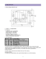
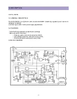
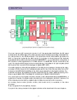
Daewoo DTU-29M5ME Service Manual Download Page 61

-60-

IC DESCRIPTION 

The base-band delay line is integrated. In devices without CVBS comb filter this delay line is
also active during NTSC to obtain a good suppression of cross colour effects. The demodulated
colour difference signals are internally supplied to the delay line. The baseband comb filter can
be switched off by means of the BPS bit (subaddress 3CH).
The subcarrier output is combined with a 3-level output switch (0 V, 2.1 V and 4.5 V). The
output level and the availability of the subcarrier signal is controlled by the CMB2-CMB0 bits.

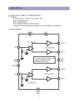
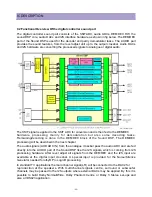
7.10 RGB output circuit

In the RGB control circuit the signal is controlled on contrast, brightness and saturation. The IC
has a YUV interface so that additional picture improvement ICs can be applied. To compensate
signal delays in the external YUV path the clamp pulse in the control circuit can be shifted by
means of the CLD bit in subaddress 44H. When the YUV interface is not required some of the
pins can be used for the insertion of RGB/YPrPb signals or as additional CVBS(Y)/C input.
When the YUV interface is not used one of the pins (VOUT) is transferred to general purpose
output switch (SWO1). The IC has also a YUV interface to th edigita ldie. Via this loop digital
features like “double window” are added.

A tint control is available for the base-band U/V signals. For this reason this tint control can be
activated for all colour standards. The signals for OSD and text are internally supplied to the
control circuit. The output signal has an amplitude of about 1.2V black-to-white at nominal input
signals and nominal settings of the various controls.

A black level off-set can be made with respect to the level which is generated by the black current stabilization
system. In this way different colour temperatures can be obtained for the bright and the dark part of the
picture. The black level control is active on the Red and the Green output signal. It is also possible to control
the black level of the Blue and the Green output signal (OFB bit = 1).

In the Vg2 adjustment mode (AVG=1) the black current stabilization system checks the output
level of the 3 channels and indicates whether the black level of the highest output is in a certain
window(WBC-bit) or below or above this window (HBC-bit). This indication can be read from the
status byte 01 and can be used for automatic adjustment of the Vg2 voltage during the
production of the TV receiver. During this test the vertical scan remains active so that the
indication of the 2 bits can be made visible on the TV screen.

The control circuit contains a beam current limiting circuit and a peak white limiting circuit. The
control is realised by means of a reduction of the contrast and brightness control settings. The way
of control (first contrast and then brightness or contrast and brightness in parallel) can be chosen by
means of the CBS bit (subaddress 44H). The peak white level is adjustable via the I2C-bus.

To prevent that the peak white limiting circuit reacts on the high frequency content of the video signal a
low-passfilter is inserted in front of the peak detector. The circuit also contains a soft-clipper which
prevents that the high frequency peaks in the output signal become too high. The difference between the
peak white limiting level and the soft clipping level is adjustable via the I2C-bus in a few steps.

During switch-off of the TV receiver a fixed beam current is generated by the black current
control circuit. This current ensures that the picture tube capacitance is discharged. During the
switch-off period the vertical deflection can be placed in an overscan position so that the
discharge is not visible on the screen.

A wide blanking pulse can be activated in the RGB outputs by means of the HBL bit in subaddress 43H.
The timing of this blanking can be adjusted by means of the bits WBF/R bits in subaddress 26H.

Summary of Contents for DTU-29M5ME

Page 1: ...L Parts Price List in Service Information Center Service Manual Color Television CHASSIS Model CM 500 500F DTU 29M5ME MP MT MZ DTU 29M6ME MP MT MZ DTU 29M7ME MP MT MZ DTU 29U1ME MP MT MZ DTU 29U5ME MP...

Page 2: ...TYPICAL SERVICE DATA 15 6 ELECTRICAL PARTS LIST 16 7 EACH MODEL PARTS LIST 24 8 SCHEMATIC DIAGRAM 25 9 PRINTED CIRCUIT BOARD 26 10 MECHANICAL EXPLODED VIEW AND PARTS LIST 29 11 IC DESCRIPTION 38 12 T...

Page 3: ...W FLAT 7 5W 7 5W at EQUILIZER CENTER Channel Conerage VHF BAND I CH 02 CH04 48 25MHz 62 25MHz BAND II CH05 CH12 175 25MHz 224 25MHz CABLE BAND S01 S03 69 25MHz 83 25MHz S01 S20 105 25MHz 294 25MHz HYP...

Page 4: ...e the picture tube to avoid the shock harzard before removing the anode cap 3 Discharge the high potential of the picture tube before handling the tube The picture tube is highly evacuated and if brok...

Page 5: ...4 3 CIRCUIT BLOCK DIAGRAM...

Page 6: ...Gunpo RND V1 01 25 11 04 Tuner option revision Byte1 bite2 1 0 V1 02 29 11 04 Curtain beep option added Byte3 bits1 Curtain ON OFF bit setting corrected V1 03 02 12 04 Local key option bit changed Dig...

Page 7: ...ervice e g SERVICE V1 00 To exit SERVICE menu press menu key or Stand By key 4 2 SERVICE MODE NAVIGATION Pr Up Down remote keys cycle through the service items available Vol remote keys Dec Increment...

Page 8: ...are two option bytes available 16 bits in all These option bits are available from FACTORY and SERVICE mode First find the OPTION1 OPTION2 or OPTION3 control and then use the UP DOWN and PLUS MINUS k...

Page 9: ...EXTING OPTION BITS MENU Push the button OPT a third time The full sequence enter to exit is FACTORY OPTION1 OPTION2 OPTION3 FACTORY 4 4 6 AFTER SETTING OPTION BITS Before pushing on the shipping key B...

Page 10: ...zoom selection in features menu WSS is also disabled Dolby Virtual Bit 3 Allows Doby Virtual trademark 3D effect to be available from the user control button 3D Note Dolby Virtual is only available w...

Page 11: ...icture setting according to the table below PARS Logo ON OFF Bit 0 Enables disables the display of PARS logo at power on 4 5 3 OPTION 3 BITS Curtain function at power ON Bit 7 Enables disables the cur...

Page 12: ...tin German East 1 0 0 Cyrillic Latin Russia East 1 0 1 Cyrillic Latin Ukrainian East 1 1 0 Latin Latin Czech Slovak East 1 1 1 Latin Latin Rumanian East Arabic 0 0 0 Latin Latin English West Persian 0...

Page 13: ...djust RED GRN and BLUE GAIN to the desired colour temperature 3 FOCUS Adjust the Focus volume on FBT to have the best resolution on screen 4 VERTICAL GEOMETRY Adjust V LINEAR linearity S CORRECT S Cor...

Page 14: ...itted on the chassis See above how to change option bits Adjust the antenna signal level at 62 dB V 2 Tune a colour bar pattern Find the AGC LEVEL item in service mode Press the key OK on the remote k...

Page 15: ...URSOR RIGHT PROGRAM DOWN CURSOR DOWN MODE OK PRESET PIP ON PIP PICTURE SWAP PIP POSITION PIP PICTURE SOURCE TV TELETEXT PIP PICTURE SIZE SLEEP ZOOM 3D SOUND EFFECT TELETEXT MODE POWER SOUND MUTE NUMBE...

Page 16: ...15 5 CM 500 F TYPICAL SERVICE DATA...

Page 17: ...TDA8358J 0000A 4857028227 HEAT SINK AL EX BK 0000B 7174301011 SCREW TAPPTITE TT2 RND 3X10 MFZN LOC PARTCODE PARTNAME DESCRIPTION REMARK I601 PTA2SW8232 HEAT SINK ASS Y 1LA42152 E 7174301011 11LA42152...

Page 18: ...LL R406 RS02Z203JS R M OXIDE FILM 2W 20K OHM J SMALL R407 RS02Z102JS R M OXIDE FILM 2W 1K OHM J SMALL R408 RF01Z100J R FUSIBLE 1W 10 OHM J TAPPING R409 RS01Z103J R M OXIDE FILM 1W 10K OHM J TAPPING R4...

Page 19: ...M14006LB TAPE MASKING 3M 232 6 0X2000M LOC PARTCODE PARTNAME DESCRIPTION REMARK 20 2TM10006LB TAPE MASKING 3M 232 MAP C 6 2X2000M A001 4859810993 PCB MAIN 330X246 D1B C101 CCZB1H102K C CERA 50V B 1000...

Page 20: ...20 RD AZ102J R CARBON FILM 1 6 1K OHM J J321 85801060GY WIRE COPPER 1 0 6 TIN COATING J405 85801060GY WIRE COPPER 1 0 6 TIN COATING J406 85801060GY WIRE COPPER 1 0 6 TIN COATING J407 85801060GY WIRE C...

Page 21: ...ING J854 85801060GY WIRE COPPER 1 0 6 TIN COATING LOC PARTCODE PARTNAME DESCRIPTION REMARK J857 85801060GY WIRE COPPER 1 0 6 TIN COATING J879 85801060GY WIRE COPPER 1 0 6 TIN COATING J888 85801060GY W...

Page 22: ...ARBON FILM 1 6 10K OHM J R739 85801060GY WIRE COPPER 1 0 6 TIN COATING LOC PARTCODE PARTNAME DESCRIPTION REMARK R740 85801060GY WIRE COPPER 1 0 6 TIN COATING R741 RD AZ101J R CARBON FILM 1 6 100 OHM J...

Page 23: ...02 COIL PEAKING 10UH K AXIAL 3 5MM LP04 5CPZ100K02 COIL PEAKING 10UH K AXIAL 3 5MM LP05 5CPZ100K02 COIL PEAKING 10UH K AXIAL 3 5MM LOC PARTCODE PARTNAME DESCRIPTION REMARK LP06 5CPZ100K02 COIL PEAKING...

Page 24: ...05 RD AZ101J R CARBON FILM 1 6 100 OHM J R906 RD AZ101J R CARBON FILM 1 6 100 OHM J R907 RD AZ101J R CARBON FILM 1 6 100 OHM J R908 RC 2Z102K R CARBON COMP 1 2 1K OHM K R909 RC 2Z102K R CARBON COMP 1...

Page 25: ...CVSNDF SV Q O C811 C CERA AC 4 0KV 2200PF M AD AC250V 4 0KV 3300PF M SD AC250V C831 C MYLAR N C 630V PU 0 047MF J D820 DIODE N C RL4A 015 308 D821 DIODE N C RL4A 015 308 J803 J804 WIRE COPPER 1 0 6 TI...

Page 26: ...25...

Page 27: ...26...

Page 28: ...27...

Page 29: ...28...

Page 30: ...29 DTU 29M5...

Page 31: ...30 DTU 29M6...

Page 32: ...31 DTU 29M7...

Page 33: ...32 DTU 29U1...

Page 34: ...RUBBER SCREW CRT FIX 4 4 CR T2 0 SWRM SK5 L 35 4852163101 COVER BACK 1 1 HIPS GY 4851114003 SIDE AV PCB PANEL AV ASSY 1 1 CM 500F CM 500F 2326802 5934301 7178301212 SCREW TAPTITE 2 TT2 WAS 3X12 MFZN...

Page 35: ...34 CM 500F 4858311110 DTU 29U8 4859645360 12W 8 SP 58126F DTU 29U8...

Page 36: ...35 DTU 29F1 CM 500F 4859845360 CPT A68AKY13X CM 500F CM 500F DTU 29F1...

Page 37: ...36 DTU 29F2 CM 500F 4859845360 CPT A68AKY13X CM 500F DTU 29F2...

Page 38: ...37 DTU 29F3 CM 500F 4859845360 CPT A68AKY13X CM 500F CM 500F DTU 29F3...

Page 39: ...together with a FLASH embedded TEXT Control Graphics m Controller TCG m Controller and US Closed Caption decoder In addition the following functions can be added Teletext decoder with 10 page text me...

Page 40: ...39 IC DESCRIPTION...

Page 41: ...0 port 2 1 or PWM0 output 12 P3 0 ADC0 port 3 0 or ADC0 input 13 P3 1 ADC1 port 3 1 or ADC1 input 14 P3 2 ADC2 port 3 2 or ADC2 input 15 P3 3 ADC3 port 3 3 or ADC3 input 16 VDDA 3 3V supply 3 3V 17 VR...

Page 42: ...ssor 5V 46 IFVO SVO CVBSI 2 IF video output selected CVBS output CVBS input 47 AUDIOIN4L audio 4 input left signal 48 AUDIOIN4R audio 4 input right signal 49 CVBS4 Y4 CVBS4 Y4 input 50 AUDIOIN2L audio...

Page 43: ...West drive output or AVL capacitor 76 VDRA vertical drive A output 77 VDRB vertical drive B output 78 VGUARD SWIO V guard input I O switch e g 4mA current sinkingcapability for direct drive of LEDs 7...

Page 44: ...ecoder Multi standard colour decoder with automatic search system and various forced mode possibilities Internal base band delay line Indication of the Signal to Noise ratio of the incoming CVBS signa...

Page 45: ...4 stereo inputs a stereo output for SCART CINCH 1 stereo output for HEADPHONE The headphone channel has an analogue volume control circuit for the L and R channel Finally 1 stereo SPEAKER output with...

Page 46: ...l Dolby Surround VDS 422 423 SRS 3D and SRS TruSurround RDS RBDS Only possible with external FM RADIO DEMOD Demodulation of the European Radio Data system RDS or the USA Radio Broadcast Data System RB...

Page 47: ...ical Blanking Interval VBI data capture of WST data Display Teletext and Enhanced OSD modes Features of level 1 5 WST and US Close Caption 50Hz 60Hz display timing modes Two page operation for 16 9 sc...

Page 48: ...tion circuis Portection from shorting to ground shorting to Vcc load shorting and overheating 2 2 BLOCK DIAGRAM 5 2 12 OUT1 IN1 Input amplifier Input amplifier Output amplifier Output amplifier Ri 20k...

Page 49: ...h single positive supply voltages The east west output stage is able to supply the sink current for a diode modulator circuit The IC is constructed in a Low Voltage DMOS LVDMOS process that combines b...

Page 50: ...cal output voltage B 5 INEW East west input voltage 6 VGND Vertical ground 7 EWGND East west ground 8 OUTEW East west output voltage 9 VFB Flyback supply voltage 10 OUTA Vertical output voltage A 11 G...

Page 51: ...slew rate of 900V ms No external components required Very simple application Single supply voltage of 200V Internal reference voltage of 2 5 V Fixed gain of 81 Black current stabilisation BCS circuit...

Page 52: ...at uses a bi directional data bus and serial clock The memory carries a built in 4 bit unique device type identifier code 1010 in accordance with the I2C bus definition Serial Clock SCL The SCL input...

Page 53: ...ators and control IC designed for flyback converter type switch mode power supply applications 6 2 FEATURES Small SIP fully isolated moulded 6 pins package Many protection functions Pulse by pulse ove...

Page 54: ...ply for control circiut 5 SS OLP Delay at Overload Soft Overload Protection and Soft Start set up Terminal Opetation Time set up 6 FB Feedback terminal Constant Voltage Control Signal Input Burst inte...

Page 55: ...oltage1 7 3 VOCPBD TH1 0 25 0 40 0 52 V Quasi Resonant Operation Threshold Voltage2 7 3 VOCPBD TH2 0 67 0 80 0 93 V FB Terminal Threshold Voltage 6 3 VFB OFF 1 32 1 45 1 58 V FB Terminal Inflow Curren...

Page 56: ...ier In this multiplier the SIF signal is converted to the intercarrier frequency by mixing it with the regenerated picture carrier from the VCO The mixer output signal is supplied to the output via a...

Page 57: ...ade with the bits SAS2 0 SO2 0 and HPO2 0 AV stereo versions without Audio DSP have no headphone output The input signal selection for the volume controlled audio outputs is realised by the HPO2 0 bit...

Page 58: ...the displayed picture the input signal of the sync separator is not derived from the various CVBS Y or RGB YPrPb inputs but from the YOUT pin For this reason the YOUT pin must be capacitively coupled...

Page 59: ...Vertical shift Vertical zoom Vertical scroll Vertical linearity correction When required the linearity setting for the upper and lower part of the screen can have a different setting Horizontal shift...

Page 60: ...a brighter impression of the picture Dynamic skin tone flesh control This function is realised in the YUV domain by detecting the colours near to the skin tone 7 9 Colour decoder The ICs decode PAL N...

Page 61: ...icture The black level control is active on the Red and the Green output signal It is also possible to control the black level of the Blue and the Green output signal OFB bit 1 In the Vg2 adjustment m...

Page 62: ...h an additional output crossbar Master volume function The control concept for the demodulator and decoder DEMDEC is based on the following new features Easy demodulator setup for all implemented stan...

Page 63: ...MSWITHNICAM Table NICAM standards Note 1 See EBU specification or equivalent specification 9 FUNCTIONAL DESCRIPTION SOUND PROCESSOR 9 1 The UOC III TV Sound Concept The UOCIII sound concept is impleme...

Page 64: ...o signal out of the AM demodulator is connected to the analogue crossbar at the video processor All other inputs to this multiplexer audio switch come from external either from a PIP frontend or SCART...

Page 65: ...Logic processing In standard TV applications the main channel signal L R will be connected to the DAC2 for reproduction at the speakers With multichannel signals centre surround or subwoofer channels...

Page 66: ...rier For NICAM demodulation a feedback signal is added to the control word of the second carrier mixer to establish a carrier frequency loop FM AND AM DEMODULATION An FM or AM input signal is fed via...

Page 67: ...728 specification After locking to the frame alignment word the data is de scrambled by applying the defined pseudo random binary sequence the NICAM decoder will then synchronize to the periodic fram...

Page 68: ...ill switch the output sound from NICAM to what ever sound is on the first sound carrier FM or AM When the error count is smaller thanthe lower error limit the NICAM sound is restored The auto mute fun...

Page 69: ...HECK REPLACE D802 D805 R803 CHECK REPLACE I802 LTV 817C CHECK VOLTAGE AT PIN I701 CHECK VOLTAGE AT PIN 21 OF I701 ST BY L POWER ON H ABNORMAL ABNORMAL NORMAL NORMAL NORMAL CHECK Horizontal AT PIN 73 O...

Page 70: ...80 OF I701 CHECK REPLACE Q502 Q503 Q504 Q505 CHECK SIGNAL AT CATHODE OF CRT CHECK REPLACE CRT BOARD CHANGE SIGNAL IF OF TUNER CHECK SIGNAL AT PIN 72 76 77 OF I701 CHECK REPLACE SCL SDA B OF I701 CHEC...

Page 71: ...HARTS CHECK SIGNAL AT 28 29 PIN OF I701 CHANGE THE SYSTEM PAL SECAM CHECK REPLACE IF OF TUNER CHECK REPLACE Z701 Z702 CHECK R G B SIGNAL 83 84 85TH OF I701 CHECK REPLACE CRT PART NORMAL NORMAL ABNORMA...

Page 72: ...OF I701 CHECK 189V Line Heater Voltage CHECK REPLACE CRT CHECK SIGNAL AT R G B INPUT AND R G B OUTPUT OF I901 CHECK REPLACE SCL SDA B OF TUNER CHECK REPLACE I701 CHECK SIGNAL AT IF OF TUNER CHECK AV S...

Page 73: ...701 CHECK REPLACE I701 CHECK REPLACE R313 R314 C313 C314 R305 R312 C305 C306 CHECK VERTICAL INPUT Vin OF I301 NORMAL NORMAL NORMAL NORMAL NORMAL ABNORMAL ABNORMAL ABNORMAL ABNORMAL CHECK VERTICAL OUTP...

Page 74: ...2 4 OF I601 CHECK SIGNAL AT PIN 57 58 I701 NORMAL NORMAL NORMAL NORMAL NORMAL ABNORMAL ABNORMAL ABNORMAL ABNORMAL CHECK SIF OUT OF I701 CHECK Speaker Connector Replade I601 CHECK REPLACE R602 R604 R6...

Page 75: ...AV2 DVD1 DVD2 CHECK SIGNAL AT PIN 49 52 55 68 69 70 OF I701 CHECK SIGNAL AT PIN R G B 83 84 85 OF I701 ABNORMAL ABNORMAL ABNORMAL NORMAL NORMAL NORMAL CHECK SIGNAL AT R G B Input and R G B Ouput of I9...

Page 76: ...G CHARTS 8 REMOTE CONTROL UNIT TROUBLE CHECK BATTERY AND LED OF REMOCON CHECK IR OF PREAMP AND VCC OF PREAMP IC IF01 CHECK REPLACE 2 nd PIN OF I701 ABNORMAL ABNORMAL NORMAL NORMAL REPLACE BATTERY REPL...

Page 77: ...DAEWOO ELECTRONICS CORP PRINTED DATE 686 AHYEON DONG MAPO GU SEOUL KOREA C P O BOX 8003 SEOUL KOREA JULY 2005...

Reviews: