14
CIRCUIT OPERATION MANUAL
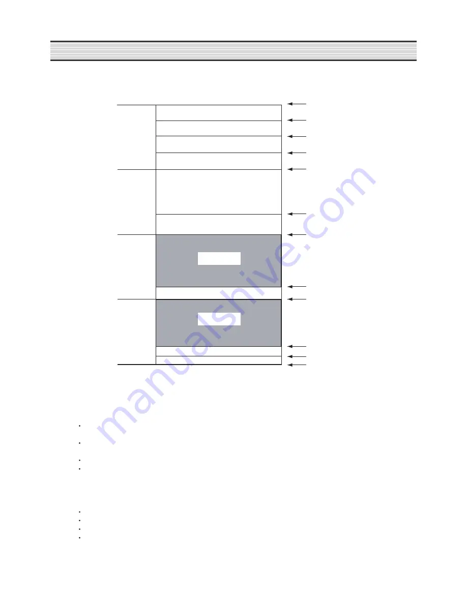
Following is the Memory MAP Table.
EMI Bank 3 (FLASH)
EMI Bank 2
EMI Bank 1
EMI Bank 0
Shared SDRAM
Peripheral configuration registers
Reglon 3
Reglon 2
Reglon 1
Reglon 0
0x70000000
0x7FFFFFFF
0x60000000
0x50000000
0x40000000
0x20040000
0x00000000
0xC0000000
0x80000800
MinInt: 0x80000000
0x80001000
0xC0300000
Not available
2 Kbyte data cache when used as SRAM
2 Kbyte SRAM
Not available
Memory Map
The size of EMI Bus is 16bit and also support for the 8bit Bus. The Bank0 of EMI can support DRAM Interface while rest of
Bank as of Bank1, 2 and 3 can only support SRAM, ROM and Peripheral Interface.
Data 0 - 15
16bit data transfer
Adr 1 - 21
When using DRAM, it supports Multiplex mode (Row and Column Address) with the access ability of 32bit.
not_WE0
not_WE1
Signals individual bite Enable Strobe when addressing 2bit word at EMI.
Not_WE0 assert : Data 0 - 7 enable
Not_WE1 assert : Data 8 - 15 enable
not_CE0
not_CE1
not_CE2
not_CE3
EMI Bank0/1/2/3 Chip select strobe
Summary of Contents for DSD-9255E
Page 17: ...16 CIRCUIT OPERATION MANUAL EMI Interface Timing...
Page 40: ...39 SCHEMATIC DIAGRAM...
Page 41: ...40 SCHEMATIC DIAGRAM...
Page 42: ...41 SCHEMATIC DIAGRAM...
Page 43: ...42 SCHEMATIC DIAGRAM...
Page 44: ...43 SCHEMATIC DIAGRAM...
Page 45: ...44 SCHEMATIC DIAGRAM...
Page 46: ...45 PARTS PLACEMENT ARRANGEMENT...
Page 47: ...46 PARTS PLACEMENT ARRANGEMENT...
Page 48: ...47 PARTS PLACEMENT ARRANGEMENT DSD 9255 FRONT DSD 9256 FRONT...
Page 49: ...48 PARTS PLACEMENT ARRANGEMENT...
Page 50: ...686 AHYEON DONG MAPO GU SEOUL KOREA C P O BOX 8003 SEOUL KOREA DAEWOO ELECTRONICS Corp...


