background image

11

CIRCUIT OPERATION MANUAL

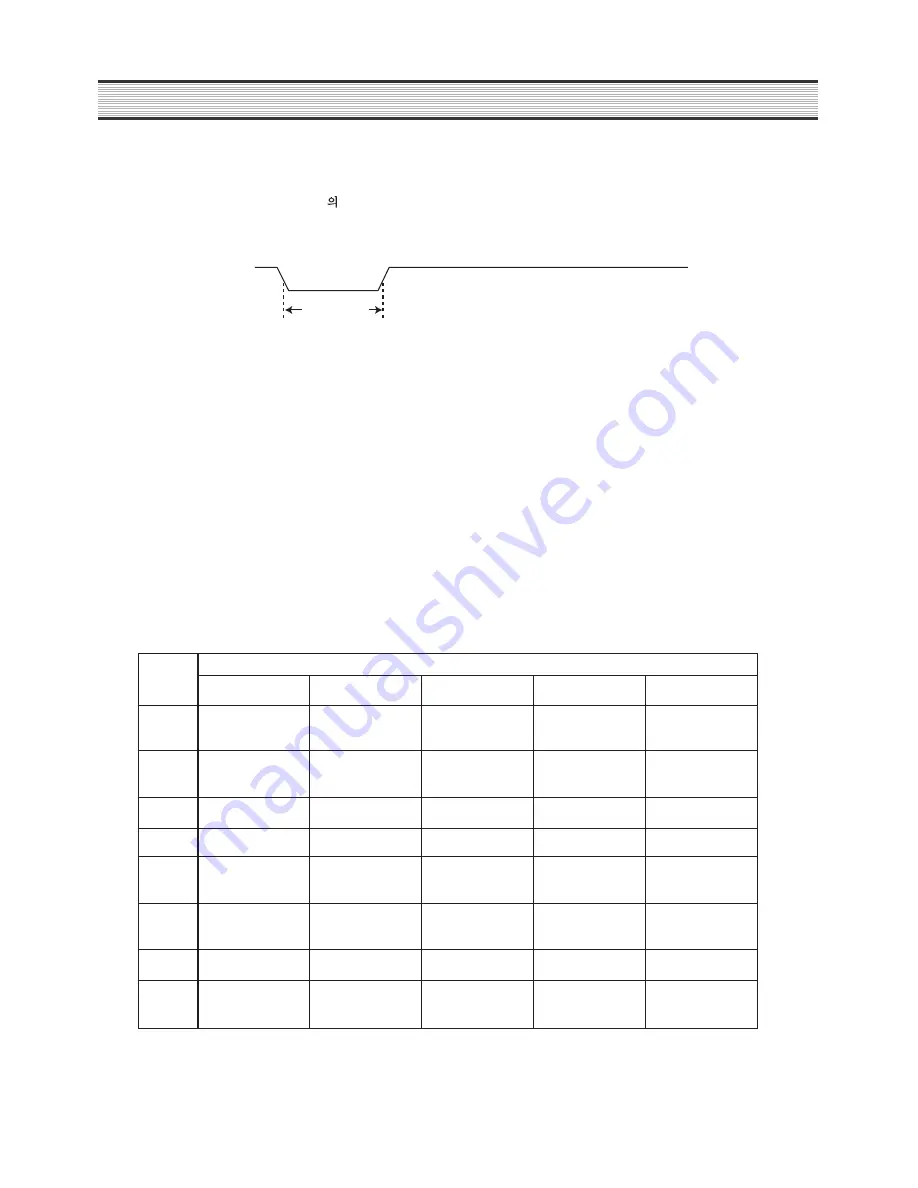
(2) Reset Section.

If the Low signal is read by Sti5518

Reset Pin, the Register value of all Sti5518 will be initialized. 

There must be at least of 8 clock (37nsec) of Reset Time.

(3) Clock Section.

STI5518 has two PLL inside. Operative clocks are made by external clock with one unit of 27MHz. The two PLL are as
of ST20 PLL and MPEG PLL.
ST20 PLL produces 81MHz of system clock that is to be used in processor and peripheral equipment.
MPEG PLL produces audio decoder system clock, audio PCM clock, TS Demultiplexer and memory clock of SDRAM.
27MHz clock uses CRYSTAL. Currency control is enabled by PWM OF Sti5518 PWM with the reference of the PCR
value of MPEG to set the exact initiative of MPEG. If this value is not appropriate the colors are not be seen on the
screen, or the screen will display broken features.

(4) PIO Structure.

Sti5518 supports PIO that back up 5 number of Ports (8bit) as of PIO0, PIO1, PIO2, PIO3 and PIO4. Some ports are
able to endow extra functions to PIO for flexible expansion in usage. Following chart shows Alternative Function Pin of
PIO.

PIO port 0

ASC0TxD or

Sc1DataOut

ASC0RxD or

Sc1DataIn

Not connected

Sc1Clk

(Sc1RST)

(Sc1CmdVcc)

ASC0Dir

(Sc1Detect)

PIO port 1

SSC0 MTSR

SSC0 MRST

SSC0 SCIK

CaptureIn1

CaptureIn2

ASC1TxD

ASC1RxD

ASC3TxD

PIO port 2

ASC2TxD

or Sc0DataOut

ASC2RxD

or Sc0DataIn

Not connected

Sc0Clk

CompareOut0

(Sc0RST)

(Sc0CmdVcc)

Not connected

CaptureIn0

(Sc0Detect)

PIO port 3

TriggerIn

TriggerOut

PIO port 4

CompareOut1

(IROut)

CaptureIn3

ASC3RxD

not_Rst

tRSTLRSTH

Min 8x37nsec

Reset Timing

Chart 2. PIO Alternate Functions.

Alternative function of PIO pins

Port bit

0

1

2

3

4

5

6

7

Summary of Contents for DSD-9255E

Page 1: ...thout notice in the parts list So if you need the latest parts information please refer to PPL Parts Price List in Service Information Center http svc dwe co kr DAEWOO ELECTRONICS Corp June 2004 http...

Page 2: ...GENERAL INFORMATION 2 CIRCUIT OPERATION MANUAL 7 FIXING ERRORS 28 BOM LIST 33 SCHEMATIC DIAGRAM 39 PARTS PLACEMENT ARRANGEMENT 45 1 CONTENTS...

Page 3: ...on Channel Management favorite move lock rename delete and sort User programmable Satellite Transponder information Automatic search for newly added transponder NIT search Stores up to 4000 channels S...

Page 4: ...he mains The apparatus shall not be exposed to dripping or splashing and that no objects filled with liquids such as vaseds shall be placed on the apparatus UNPACKING 1 x Remote Control Unit RCU 1 x R...

Page 5: ...e selected item in the menu screen or enters the Desired value in any input mode Returns to the previous menu or exit window Moves up down a page in the channel list Executes sort or deletion of satel...

Page 6: ...Optic jack Optional function Connect Video to a TV using RCA jack Connect Audio L R to TV or Audio device Serial Connect to a PC for S W upgrade Loopthrough LNB IN Connect to Satellite Antenna To move...

Page 7: ...n Level Resolution 720 x 576 pixels for PAL Aspect ratio 4 3 or 16 9 Audio format MPEG Layer I and II Channel Mode Stereo Mono Mode Audio Signal Sample Rate 32 44 1 48 Ksps Audio Signal bandwidth 15Hz...

Page 8: ...AM DSD 9280M Block Diagram CPU STi5518 AUDIO D A FLASH ROM 16Mbit SDRAM 64Mbit Television Satellite dish TUNER A D 6bit DUAL LINK IC QPSK FEC TV SCART RCA RS 232 PORT VIDEO AUDIO FRONT SMPS 5V 3 3V 12...

Page 9: ...0100 0000 K03 3 E8 H 03 H 0001 0111 1100 0000 K04 4 E8 H 04 H 0001 0111 0010 0000 K05 5 E8 H 05 H 0001 0111 1010 0000 K06 6 E8 H 06 H 0001 0111 0110 0000 K07 7 E8 H 07 H 0001 0111 1110 0000 K08 8 E8...

Page 10: ...E8 H 00 H 0001 0111 0000 0000 K18 9 E8 H 09 H 0001 0111 1001 0000 K19 E8 H 12 H 0001 0111 0100 1000 K20 OK E8 H 11 H 0001 0111 1000 1000 K23 EPG E8 H 24 H 0001 0111 0010 0100 K28 YELLOW E8 H 29 H 0001...

Page 11: ...ories 4 Banks Able to use Hardware DMUX input Serial and to support 32Pid Boosting 8 Level INT Supporting DMA and other multi PID 2 MPEG DMAs Serial IEEE 1394 Hardware transport strearn demux 2 Kbytes...

Page 12: ...f this value is not appropriate the colors are not be seen on the screen or the screen will display broken features 4 PIO Structure Sti5518 supports PIO that back up 5 number of Ports 8bit as of PIO0...

Page 13: ...data Latch data Transmit data Feature 7 I2 C Timing Chart 3 PIO Map PIO NAME I O Function Remarks PIO1_0 I2C_Data SSC0 I O PIO1_2 I2C_Clk O PIO1_3 NOTPGM_EN O L Flash program enable PIO1_4 SLOW_S W I...

Page 14: ...n in High status and Key Scan Trigger IN PIO3_6 Trigger OUT PIO3_7 Used when debugging with DCU Tool REMOCON_IN PIO4_6 Recognize the REMOCON signal being sent from IR Sensor 5 Memory Interface Sti5518...

Page 15: ...Kbyte SRAM Not available Memory Map The size of EMI Bus is 16bit and also support for the 8bit Bus The Bank0 of EMI can support DRAM Interface while rest of Bank as of Bank1 2 and 3 can only support S...

Page 16: ...ce Clock high to Strobe Valid 8 0 0 0 ns tRCA CH Read Data valid to Reference Clock high 13 0 ns tCHRDX Read Data hold after Reference Clock high 2 0 ns tSVRDX Read Data hold after Strobe valid 0 0 ns...

Page 17: ...16 CIRCUIT OPERATION MANUAL EMI Interface Timing...

Page 18: ...Demodulator are combined into one Module Following feature shows the Block Diagram 2 WIRE BUS CONTROL Direct conversion ZIF Tuner 4MHz 4MHz TDA8260 INSIDE LPF Matched Filter Matched Filter 2 wire bus...

Page 19: ...R INPUT OF LNB A 2 NC 3 5V RF 5V OF RF AMP 20mA TYP 20mVp p 4 AGC AGC MONITORING 5 5V 5V OF 2 nd AMP ZERO IF IC 20mA TYP 20mVp p 6 GND 7 VT TUNING VOLTAGE 30V 20mVp p 8 I I SIGNAL MONITORING 9 Q Q SIG...

Page 20: ...ith LNB 1 LNB power and 22khz Tone Pulse The power supplied to LNB sends the 22Khz Tone signal that is used in horizontal 18V vertical 13V and frequency Band and Diseqc Command Chart 6 LNB Control sig...

Page 21: ...rts Interlace mode or Non interlace mode There are 6 Pins for the Analogue Video output CVBS S VHS Y C RGB Moreover it supports Teletext closed captions and CGMS Following picture shows the signal for...

Page 22: ...0 0 00 0 000 White Yellow Cyan Green Magenta Red Blue Block 400 388 316 284 238 204 152 BLACK BLANK WHITE LEVEL LEVEL SYNC IFVFI Color Burst 10 Cycles Maintain 300mV Maintain 300mV White Yellow Cyan G...

Page 23: ...Pin that are used in the DSD 9255M is as following Chart 9 Slow Fast Blanking Function Chart 70 TV SCART Connector Pin SCART CONNENTOR Following Table shows the Scart Connector Can select either TV A...

Page 24: ...systems PCM1754 Texas Instruments Following diagram shows Timing Diagram with Audio DAC and TI PCM1754 Block 2 Audio Pin Name Description Singnal Level Impedance 1 2 3 4 5 6 7 8 9 10 11 12 13 14 15 16...

Page 25: ...SPDIF Format Use PCM1754 Texas Instruments which are IC of the Digital Audio Encoding system in SPDIF format The signals are entered from the PCM Format I2S Format The Digital Signals that were encode...

Page 26: ...read write by PC 2 sign is displayed in Front Panel Check whether the User Data is being loaded to Main RAM from the Flash ROM Check the validity of Data Following Booting Message will be seen after e...

Page 27: ...r Initial TUNER Module Initialization Creating TUNER module semaphores module_type 148 Successfully Installed TUNER module 5 MPEG SDRAM configuration MPEG SDRAM configuration Video Bit Buffer Size 400...

Page 28: ...serivce_num 0 LOAD POSt parsing process start LOAD POSt parsing process start LOAD POSt parsing process start LOAD POSt parsing process start LOAD POSt parsing process start Last Channel didn t save b...

Page 29: ...rcuit Oscillating 27Mhz clock Flash Cs output status Check CPU power STi5518 Pin27 High Check ROM Booting Mode Check Wait Signal STi5518 Pin131 Low Eliminate the problems Replacing STI5518 BUS Interfa...

Page 30: ...ol LNBP output OK IC27 PIN3 Eliminate problem causing factors Replace LNBP Check the power of LNB 13V 18V 12C Line Check Reset Check Check Locking Voltage 1 16V Tuner PIN 13 near TP Replace Tuner B Ch...

Page 31: ...the problem Check Error Pin Whether the output is in High Status Replace Tuner Tuner interface Signal check TS_Data F_packet_clk F_strt F_B_clk Fix the problem Pts Crystal Check Stream Input Signal c...

Page 32: ...put Signal PCM Data SCLK LRCLK PCMCLK YES NO YES NO NO Check the STi 5518 Check the Interface OF Audio AMP IC Replace STi5518 Replace Audio DAC Eliminate problems Replace Audio AMP Audio AMP Check Aud...

Page 33: ...s Check the power status of Sit5518 Video Pin 23 Pin30 Check Related Circuits and execute the fixing process Replace STi5518 I V Ref Check STi5518 Pin28 29 Pin35 36 Verify the resistance value and per...

Page 34: ...R0 1MFK1608 C106 HCBK103KBA CCHIPCERA 50VX7R0 01MFK1608 C107 HCBK104KBA CCHIPCERA 50VX7R0 1MFK1608 C108 HCBK222KBA CCHIPCERA 50VX7R2200PFK1608 C110 HCBK104KBA CCHIPCERA 50VX7R0 1MFK1608 LOC PARTS_CODE...

Page 35: ...T FM809TS3 IC305 1ST232CD Q ICCHIPDRIVE ST232CD IC401 1ST15518BQ ICCHIPDECODER STI5518BVC208PINPQFP IC402 1160ATTC7Q ICCHIPFLASHROM MX29LV160ATTC 7048PINTSOP IC403 1T436416AT ICCHIPSDRAM T436416A 7S L...

Page 36: ...HRFS822JBA RCHIP 1 16 8 2KOHMJ1608 R229 HRFS750JBA RCHIP 1 1675OHMJ1608 R230 HRFS271JBA RCHIP 1 16 270OHMJ1608 LOC PARTS_CODE PARTS_NAME PARTS_DESCR REMARK R231 HRFS750JBA RCHIP 1 1675OHMJ1608 R232 H...

Page 37: ...BA RCHIP 1 16 0OHM1608 R452 HRFS000 BA RCHIP 1 16 0OHM1608 LOC PARTS_CODE PARTS_NAME PARTS_DESCR REMARK R601 HRFS101JBA RCHIP 1 16 100OHMJ1608 R602 HRFS103JBA RCHIP 1 16 10KOHMJ1608 R603 HRFS103JBA RC...

Page 38: ...WIRECOPPER AWG221 0 65TINCOATING JP708 85801065GY WIRECOPPER AWG221 0 65TINCOATING LOC PARTS_CODE PARTS_NAME PARTS_DESCR REMARK R723 RD AZ330J RCARBONFILM 1 633OHMJ R724 RD AZ560J RCARBONFILM 1 656OH...

Page 39: ...DZUZ5R6BSB DIODEZENER UZ 5 6BSB 5 46 5 70V D819 DZN4004S DIODE 1N4004S AUT0 D821 DZN4004S DIODE 1N4004S AUT0 LOC PARTS_CODE PARTS_NAME PARTS_DESCR REMARK JP801 85801065GY WIRECOPPER AWG221 0 65TINCOA...

Page 40: ...39 SCHEMATIC DIAGRAM...

Page 41: ...40 SCHEMATIC DIAGRAM...

Page 42: ...41 SCHEMATIC DIAGRAM...

Page 43: ...42 SCHEMATIC DIAGRAM...

Page 44: ...43 SCHEMATIC DIAGRAM...

Page 45: ...44 SCHEMATIC DIAGRAM...

Page 46: ...45 PARTS PLACEMENT ARRANGEMENT...

Page 47: ...46 PARTS PLACEMENT ARRANGEMENT...

Page 48: ...47 PARTS PLACEMENT ARRANGEMENT DSD 9255 FRONT DSD 9256 FRONT...

Page 49: ...48 PARTS PLACEMENT ARRANGEMENT...

Page 50: ...686 AHYEON DONG MAPO GU SEOUL KOREA C P O BOX 8003 SEOUL KOREA DAEWOO ELECTRONICS Corp...

Reviews: