16
CIRCUIT OPERATIONAL DESCRIPTION
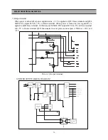
7) Output terminal
When power is turned off at power applied status, +3.3V is applied to Q822 Base terminal and Q824
MOS FET outputs MVCC(+5V) to Drain terminal. When power is turned on, low signal(0V) is
applied to Q822 Base terminal. At this time, Q824 MOS FET outputs MVCC(+5V) to Drain terminal
and +5V to Source terminal. Q823 funcionates in same process and o12M(Ever +12V) and
+12V.
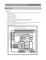
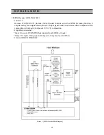
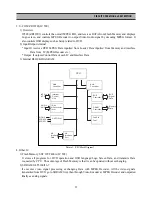
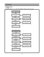
2. POWER SUPPLY BLOCK DIAGRAM
NOISE
FILTER
SUNBBER
Switching
Primary
rectification
voltage
Control Drive
Circuit
Costant-voltage
Control Drive
Circuit
Starting
Part
Secondery
rectification
voltage
Picture
7 [
Output terminal
]
Summary of Contents for DQD-2100D
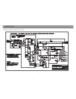
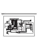
Page 5: ...4 CIRCUIT DIAGRAM POWER SUPPLY SCHEMATIC DIAGRAM DQD 6100 220V ...
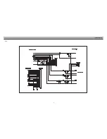
Page 6: ...5 CIRCUIT DIAGRAM VIDEO ...
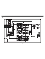
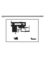
Page 7: ...6 CIRCUIT DIAGRAM AUDIO ...
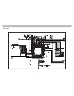
Page 8: ...7 CIRCUIT DIAGRAM VFD JOG ...
Page 9: ...8 CIRCUIT DIAGRAM ETC ...
Page 10: ...9 CIRCUIT DIAGRAM VCR_INT DVD ...
Page 11: ...10 CIRCUIT DIAGRAM ATAPI DVD ...
Page 12: ...11 CIRCUIT DIAGRAM CPU ZR36703 DVD ...
Page 13: ...12 CIRCUIT DIAGRAM MPEG DECODER ...
Page 46: ...45 COMPONENTS LOCATION GUIDE ON PCB BOTTOM VIEW ...
Page 47: ...46 JOG COMPONENTS LOCATION GUIDE ON PCB BOTTOM VIEW M P E G ...
Page 48: ...47 DISASSEMBLY ...
Page 49: ...48 DISASSEMBLY ...
Page 50: ...49 DISASSEMBLY ...
Page 51: ...50 DISASSEMBLY ...

