background image

Service manual SC-150

-52-

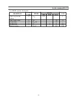
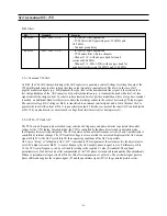
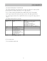
configuration

Stand by

TV ON

1

Power

Push Pull Low

Push Pull High

Switch OFF / ON SMPS

2

AGC

High impedance

High impedance

Tuner AGC level input –
For factory use only

5

Mod SW

High impedance

Push Pull

High = Negative
modulation, Low = Positive
modulation (L/L’).

6

SECAM L’

High impedance

Push Pull

Low = L, High =L’

7

AFC

High impedance

High impedance

ADC input

8

IR

High impedance

High impedance

Interrupt input

9

SC1 SW

High impedance

High impedance

SCART 1 slow switching –
ADC input

10

SC2 SW

High impedance

High impedance

SCART 2 slow switching –
ADC input

61

Mute

Push Pull

Push Pull

High = Mute active

62

LED

Open Drain

Open Drain

63

KB

High impedance

High impedance

Keyboard input – ADC
input

64

OCP

High impedance

High impedance

Over Current Protection –
Switch the set to Std by if < 2.

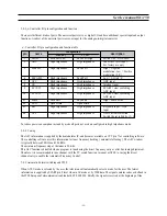
5-4-3   - Controller I/O pin configuration and function

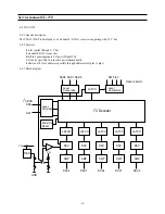
There exist different kinds of ports. The universal ports serve as digital I/O and have additional special input and output
functions. A subset of the universal ports serves as input for the analogue-to-digital converter.

   - Controller I/O pin configuration and function table

pin

name

description

To reduce power consumption in stand by mode all ports not used are configured in high impedance mode.

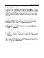
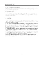
5-4-4  Tuning

The AFC information is supplied by the demodulator IC, and becomes available on VCT pin 7 for controlling software.
The controlling software uses this information for tuner frequency tracking ( automatic following ). The AFC window
is typically between 50 KHz and 100 KHz.
The minimum frequency step of the tuner is 50 Khz.
This AFC function is disabled when a program is tuned using the direct frequency entry or after fine tuning adjustment.
Therefore it is recommended to tune channel with the TV search function ( manual or ATSS ) or using the direct
channel entry to enable the Automatic Frequency Control.

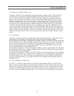
5-4-5 Automatic Format switching and WSS

When AUTO mode is selected by the user, the television will automatically select a mode for the user. The format
information is supplied by SCART pin 8 level when in AV mode or by WSS data. The signal contains codes as defined in
the WSS European Telecommunication Standard, ETS 300 294. Briefly, the signal is received at the beginning of line

Summary of Contents for CHASSIS : SC-150 Model : DSC-3220E

Page 1: ...Service Manual Color Television CHASSIS SC 150 Model DSC 3220E 3220L S M No DSC150BEF0 DEC 2002 DAEWOO ELECTRONICS Corp http svc dwe co kr...

Page 2: ...nal processor Teletext decoder with embedded 8 bit Controller 18 4 1 1 Block diagram off the VCT 18 4 1 2 TV signal Processor 18 4 1 2 Controller 19 4 1 4 Teletext Features 19 4 1 5 Displaty OSD Featu...

Page 3: ...iagram 43 43 5 2 IF section 44 5 2 1 Block diagram 44 5 2 2 Vision IF Amplifier 44 5 2 3 Tuner andVIF ACG 45 5 2 4 FPLL VCO and AFC 45 5 2 5 Video Demodulation and Amplifier 46 5 5 6 Sound IF Amplifie...

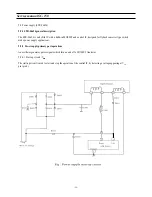
Page 4: ...sistor 58 5 8 5 EAST WEST Amplifier TD A8358J only 58 5 9 P ower supply STR F6653 59 5 9 1 STR F6654 gener aral descr iption 59 5 9 2 Power supply primary part operations 59 5 10TV start up TV normal...

Page 5: ...rage Off air channels S cable channels and hyperband Tuning system frequency synthesiser tuning system Visual screen 32 76Cm Channel indication On Screen Display program Selection 100 programmes Aux t...

Page 6: ...Italian Spanish Dutch Danish Finnish Norwegian Swedish Greek Polish Czech Slovakian Romanian Russian Bulgarian Hungarian Philips Alps Partsnic 3411G Off Spatial Panorama Dolby Virtual SC 150 VCT Versi...

Page 7: ...p 0 1V Impedance 75 16 Fast Switching 0 to 0 4V Logic 0 1 to 3V Logic 1 Impedance 75 17 Video Out Earth 18 Video In Earth 19 Video Output 1 Vpp 3dB Impedance 75 20 Video Input 1 Vpp 3dB Impedance 75 2...

Page 8: ...Service manual SC 150 7 19 Video Output 1 Vpp 3dB Impedance 75 Monitor output Not available for cp885 20 Video Input Y In 1 Vpp 3dB Impedance 75 21 Common Earth...

Page 9: ...C18 192 25 85 75 C19 201 25 C20 C21 471 25 471 25 471 25 471 25 C22 479 25 479 25 479 25 479 25 C23 487 25 487 25 487 25 487 25 C24 495 25 495 25 495 25 495 25 C25 503 25 503 25 503 25 503 25 C26 511...

Page 10: ...25 C58 767 25 767 25 767 25 767 25 C59 775 25 775 25 775 25 775 25 C60 783 25 783 25 783 25 783 25 C61 791 25 791 25 791 25 791 25 C62 799 25 799 25 799 25 799 25 C63 807 25 807 25 807 25 807 25 C64 8...

Page 11: ...25 311 25 311 25 S23 319 25 319 25 319 25 319 25 S24 327 25 327 25 327 25 327 25 S25 335 25 335 25 335 25 335 25 S26 343 25 343 25 343 25 343 25 S27 351 25 351 25 351 25 351 25 S28 359 25 359 25 359 2...

Page 12: ...from the selected country and named by the TV controlling softw are Within this group the sorting order is fixed by the A TSS list Group II It contains all the pro grams with a strong signal strength...

Page 13: ...odulation and then a second time with France system selected positive video modulation Special case GB Note for sa tellite recei ver users Before starting ATSS tur n On your satellite r ecei ver and t...

Page 14: ...equipment 2 Discharge the high potential of the picture tube before handling the tube The picture tube is highly evacuated and if broken glass fragments will be violently expelled 2 If any Fuse in thi...

Page 15: ...press menu key or Std By key 3 2 Service mode navigation Pr Up Down remote keys cycle through the service items available Vol remote keys Decrement Increment the values within range 0 7 digit keys Tog...

Page 16: ...tion fron the nominal channel frequency Find AFT item in service mode Adjust the coil L150 to bring the cursor to central position 32 3 4 2 G2 alignment Tune a colour bar pattern Find the G2 SCREEN it...

Page 17: ...zontal picture centring Adjust HOR CEN Horizontal center to have the picture in the center of the screen 3 4 7 Eau West comection Adjust the PARABOLA HOR WIDTH CORNER HOR PARAL EW TRAPEZ H BOW to comp...

Page 18: ...ual SC 150 17 CORNER EW TRAPEZ 3 4 8 AGC Adjust the antenna signal level at 70 dB V 2 Tune a colour bar pattern Find the AGC item in service mode Adjust AGC volume RB10 to bring the cursor to central...

Page 19: ...tor VIN VRT SGND VSUPAF GNDAF VSUPD GNDD VERT EW PROT HOUT HFLB SENSE RSW GNDM VRD XREF Video Front end Comb Filter Color Decoder Panorama Scaler Display Processor Pict Improv Video Back end Audio CIN...

Page 20: ...apture compare module watchdog timer 14 bit PWM for voltage synthesis Four 8 bit PWMs 10 bit ADC with 15 1 input MUX I2C bus master interface 24 programmable I O ports 80C51 controller core standard i...

Page 21: ...nking Signal CVBS and from this extracts the required data which is then decoded and stored in memory The extraction of the data is performed in the digital domain The first stage is to select and con...

Page 22: ...es Adaptive Comb filter Panorama Scaler 4 1 11 IC marking and version Chassis OSD languages ATSS countries Text SC 150 VCT3834A Pan European Latin Cyrillic Greek GB France Germany Italy Belgium Spain...

Page 23: ...tooth Output 36 EW OUT Vertical Parabola Output 37 SENSE IN SenseADC Input 38 GNDM SUPPLY Ground MADC Input 39 RSW1 OUT Range Switch1 for MeasurementADC 40 RSW2 OUT Range Switch2 for MeasurementADC 41...

Page 24: ...3 3V GND GND GND XREF VRD GND 5V B out G out R out SVM out RSW2 RSW1 GND SENSE EW VERTQ VERT HFLB Power 1 2 3 4 5 7 8 9 10 17 19 20 21 22 23 24 25 26 27 28 29 31 30 32 18 11 12 13 14 15 16 6 AGC S B...

Page 25: ...terrestrial TV sound standards Precise bit error rate indication Automatic switching from NICAM to FM AM or vice versa Improved NICAM synchronisation algorithm Improved carrier mute algorithm Improved...

Page 26: ...ian Spanish and French TV standards high quality stereo sound is transmitted digitally The systems allow two high quality digital sound channels to be added to the already existing FM AM channel The s...

Page 27: ...on Pin No Pin Name Type Short description 1 TP Out Test pin 2 NC Not Connected 3 NC Not Connected 4 TP Out Test pin 5 TP Out Test pin 6 ADR_SEL In I2C bus Address select 7 STANDBYQ In Standby Low acti...

Page 28: ...Reference ground 1 high voltage part 36 SC1_OUT_R Out Scart output 1 right 37 SC1_OUT_L Out Scart output 1 left 38 NC Not Connected 39 AHVSUP Analog power supply 8 0V 40 CAPL_M Volume capacitor MAIN 4...

Page 29: ...es Alignment free AFC without external reference circuit polarity of the AFC curve is switchable VIF AGC for negative modulated signals peak sync detection and for positive modulation peak white black...

Page 30: ...SIF2 SIF2 input symmetrical 4 3 4 Block diagram Offset 26 18 20 21 14 VCO l switch VCO Control phase shift FPLL VIF amp Loop filter comp optional 4 9 16 AM det FM det 25 24 17 Cref 23 13 22 19 6 7 8 1...

Page 31: ...supply voltage channel 2 positive loudspeaker terminal 2 GND2 Vcc2 OUT2 positive input2 4 4 TDA8946J Stereo AudioAmplif ier The TDA8946J is a dual channel audio po wer amplifier with an output power...

Page 32: ...3 14 15 16 17 4 5 TDA8358J Vertical Amplifier The TDA8358J are power circuit for use in 90o and 110o colour deflection systems for field frequencies of 25 to 200Hz and 16 9 picture tubes The circuit p...

Page 33: ...urrent from the diode modulator circuit Features Few external components Highly efficient fully DC coupled vertical output bridge circuit Short rise and fall time of the vertical flyback switch Guard...

Page 34: ...pical bandwidth of 5 5 MHz for an output signal of 60 Vpp High slew rate of 900V s No external components required Very simple application Single supply voltage of 200V Internal reference voltage of 2...

Page 35: ...Service manual SC 150 34 Block diagram TDA6107Q...

Page 36: ...erial clock 7 WC Write control 8 Vcc Supply voltage 4 Vss Ground The memory device is compatible with the I2C memory standard This is a two wire serial interface that uses a bi directionnal data bus a...

Page 37: ...nd control IC designed for flyback converter type switch mode power supply applications 4 8 2 Features Small SIP fully isolated molded 5 pins package Many protection functions Pulse by pulse overcurre...

Page 38: ...Circuit current in 4 5 IIN on 30 mA operation Circuit current in non 4 5 IIN off 100 mA A operation Maximum OFF time TOFF max 45 55 SEC Minimum time for input of 1 5 TTH 2 1 0 SEC quaxi resonant signa...

Page 39: ...ectrical characteristics IC PINS RATING NUMBER MIN TYPE MAX Drain to source break 3 2 VDSS 650 V voltage Drain leakage current 3 2 IDSS 300 A On resistance 3 2 RDS on 1 95 Switching time 3 2 tf 2 50 n...

Page 40: ...4general purpose I O ports Digital I O I O can be specified to respective ports independently Selection of 8 slave addresses possible through address select pins 3 pins 4 9 3 Block diagram Level Conve...

Page 41: ...e I O port 1 SW1 2 SW0 VILmax 1 5V 9 SW2 VIHmin 3V 10 SW3 VOLmax 0 4V 10 GND 11 SDA0 GND pin 12 SDA1 13 SDA2 15 SCL Slave address input pin Input at positive logic VILmax 1 5V VIHmin 3V SCL input pin...

Page 42: ...n Mute function Current consumption 5 1mA typ Operating power supply voltage range 4 6 13 0V Frequency response 10MHz Crosstalk 64dB at 4 43MHz 4 10 3 Block diagram 4 10 4 Pin Description 1 2 3 4 5 6...

Page 43: ...e in 10 pin SIPs and operates from 15V and 15V supplies 4 11 2 Features 0 5A output current 100dB voltage gain 80dB common mode rejection 0 15V us slew rate 4 11 3 Block diagram 2mV offset voltage 10n...

Page 44: ...Service manual SC 150 43 5 Circuit description 5 1 Block diagram...

Page 45: ...tial input Pin 6 7 of the VIF amplifier 5 2 2 Vision IF Amplifier This amplifier consists of three AC coupled amplifier stages Each differential amplifier is gain controlled by the automatic gain cont...

Page 46: ...ner AGC to generate the tuner AGC current at Pin 11 open collector output The take over point of the tuner AGC can be adjusted at Pin 10 by a potentiometer or an external dc voltage from interface cir...

Page 47: ...AGC is related to the average level of AM or FM carrier and controls the SIF amplifier to provide a constant SIF signal to the AM demodulator and QPS mixer 5 2 7 Quasi Parallel Sound QPS Mixer The QPS...

Page 48: ...rier chrominance signal These inputs are internally biased and have a fixed gain amplifier 5 3 4 Clamping The composite video input signals are AC coupled to the IC The clamping voltage is stored on t...

Page 49: ...lour standards The colour killer uses the burst phase burst frequency measurement to identify a PAL NTSC or SECAM colour signal For PAL NTSC the colour is switched off killed as long as the colour sub...

Page 50: ...b signals are converted by a program mable matrix to RGB colour space The digital OSD insertion circuit allows the insertion of a 5 bit OSD signal The OSD signals and the display clock are synchronis...

Page 51: ...o BCL limited drives and brightness 5 3 17 Analogue RGB Insertion The VCT 38xxA allows insertion of external analogue RGB signals The RGB signal is key clamped and inserted into the main RGB by the Fa...

Page 52: ...cuitry VSUP D 5 4 Microcontroller 5 4 1 Introduction The TV controller basically consists of the CPU RAM ROM and a number of peripheral modules For instance a memory banking module is included to allo...

Page 53: ...s as input for the analogue to digital converter Controller I O pin configuration and function table pin name description To reduce power consumption in stand by mode all ports not used are configured...

Page 54: ...mall horizontal geometrical error typically 8 linear ZOOM 16 9 133 100 Picture is displayed 16 9 picture letter box filling the full screen format with 430 active width and height lines PANORAMA 100 1...

Page 55: ...CART AV 2 input does not possess a FAST SWITCHING input The HIGH state of a slow switching input represents the request from the external source to be selected by the television Whether this is accept...

Page 56: ...en broadcaster the intended language that the teletext page should be displayed in As there are only 3 bits there are only 8 codes available to cover all the possible language combinations This means...

Page 57: ...Danish Finnish Norwegian Swedish Greek Polish Hungarian Czech Slovakian Rumanial Russian Bulgarian 5 6 Sound processing 5 6 1 Analogue sound IF input section The input pins ANA_IN1 and ANA_IN offer th...

Page 58: ...signal quality and automatically switches to the analogue sound carrier 1 if the transmission quality is too poor To avoid unwanted automatic switching the threshold levels mono to stereo and stereo...

Page 59: ...through the deflection coils measured as voltage across R398 which provides internal feedback information The voltage across R398 is proportional to the output current 5 8 1 Flyback voltage The flybac...

Page 60: ...designed for flyback converter type switch mode power supply applications 5 9 2 Power supply primary part operations An oscillator generates pulses signals which turn on and off a MOSFET transistor 5...

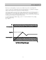
Page 61: ...does not increase to the set voltage immediately after the control circuit starts operating VIN starts dropping However as this winding voltage reaches the set value before VIN voltage drops to the s...

Page 62: ...Service manual SC 150 61 5 9 2 2 STR F6654 oscillating operation...

Page 63: ...by C1 and R1 is the OFF time of the MOSFET When C1 voltage falls to around 3 7V the STR F6654 internal oscillator is reversed again and the MOSFET turns ON C1 is quickly charged to around 6 5V The MO...

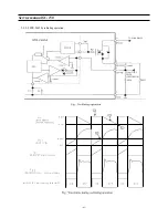
Page 64: ...ulator This regulator provides 5V 3 3V DC voltage to I501 microcontroller power supply pins pin 3 pin 54 and to the reset pulse circuit which provides reset pulse to I501 microcontroller reset pin pin...

Page 65: ...hing off the microcontroller switches TV set to stand by mode decreasing power pin voltage pin 1 5 10 2 TV normal run and stand by mode operations Depending on remote control commands I501 microcontro...

Page 66: ...he ground and I810 controlled rectifier gate pin is set to low no conducting So current from 14V DC voltage from T801 SMPS transformer pin 13 does not flow through Q811 and Q810 transistors but flows...

Page 67: ...udes an IC error amplifier I806 which corrects unexpected DC voltage variations on this line power supply IC delivery during TV set normal run power supply line IC power supply delivery Remarks 143V F...

Page 68: ...C H I N G C I R C U I T T801 SM PS TRA N S I501 M A I N IC OCP FB D801 D804 GRAETZ BRIDGE 16 D821 I810 controlled rectifier HIGH C841 C840 R713 1 3 1 2 61 64 56 54 7 63 CONDUCTING I R I N com supply...

Page 69: ...ier gate pin is set to high and I810 is conducting So current flows from pin 16 SMPS transformer to the ground via I804 optocoupler and Q810 and Q811 transistors which are conducting In these conditio...

Page 70: ...C ELECTRO 50V RHD 6 8MF 16X35 5 C801 CL1UC3474M C LINE ACROSS 0 47MF 1J UCVSNDF SV Q O C805 CEYN2G181P C ELECTRO 400V LHS 180MF 25X35 C812 CH1BFE472M C CERA AC AC400V 4700PF M U C V C813 CEXF2E101V C...

Page 71: ...LET BSR T0 2 R2 3 E015 4856310600 EYE LET BSR T0 2 R2 3 E016 4856310600 EYE LET BSR T0 2 R2 3 E017 4856310600 EYE LET BSR T0 2 R2 3 z_loc z_parts_code parts_name parts_descr E018 4856310300 EYE LET BS...

Page 72: ...5X11 TP C614 CEXF1H109V C ELECTRO 50V RSS 1MF 5X11 TP C615 CEXF1H109V C ELECTRO 50V RSS 1MF 5X11 TP C616 CEXF1H100V C ELECTRO 50V RSS 10MF 5X11 TP C619 CEXF1E221V C ELECTRO 25V RSS 220MF 8X11 5 TP z_...

Page 73: ...CBZF1H104Z C CERA SEMI 50V F 0 1MF Z C528 CCZF1H223Z C CERA 50V F 0 022MF Z C529 CCZF1H223Z C CERA 50V F 0 022MF Z C530 CCZF1H223Z C CERA 50V F 0 022MF Z C534 CCZB1H333K C CERA 50V B 0 033MF K AXL C5...

Page 74: ...1BM DA08 DUZ5R6BM DIODE ZENER UZ 5 6BM DA09 DUZ5R6BM DIODE ZENER UZ 5 6BM DA1 DUZ5R1BM DIODE ZENER UZ 5 1BM DA10 DUZ5R6BM DIODE ZENER UZ 5 6BM DA11 DUZ5R6BM DIODE ZENER UZ 5 6BM DA15 DUZ5R6BM DIODE Z...

Page 75: ...OPPER AWG22 1 0 65 TIN COATING J187 85801065GY WIRE COPPER AWG22 1 0 65 TIN COATING J188 85801065GY WIRE COPPER AWG22 1 0 65 TIN COATING J189 85801065GY WIRE COPPER AWG22 1 0 65 TIN COATING J190 85801...

Page 76: ...RD AZ101J R CARBON FILM 1 6 100 OHM J R541 RD AZ122J R CARBON FILM 1 6 1 2K OHM J R542 RD AZ303J R CARBON FILM 1 6 30K OHM J z_loc z_parts_code parts_name parts_descr R543 RD AZ241J R CARBON FILM 1 6...

Page 77: ...OHM J RA09 RD AZ750J R CARBON FILM 1 6 75 OHM J RA10 RD AZ101J R CARBON FILM 1 6 100 OHM J RA11 RD AZ750J R CARBON FILM 1 6 75 OHM J z_loc z_parts_code parts_name parts_descr RA12 RD AZ750J R CARBON...

Page 78: ...CBZF1H104Z C CERA SEMI 50V F 0 1MF Z CT05 CBZF1H104Z C CERA SEMI 50V F 0 1MF Z CZ01 CCZB1H561K C CERA 50V B 560PF K z_loc z_parts_code parts_name parts_descr CZ02 CCZB1H561K C CERA 50V B 560PF K D911...

Page 79: ...HM J RT09 RD AZ222J R CARBON FILM 1 6 2 2K OHM J RT10 RD AZ103J R CARBON FILM 1 6 10K OHM J z_loc z_parts_code parts_name parts_descr RF27 RD 4Z221J R CARBON FILM 1 4 220 OHM J RT01 RD 2Z100J R CARBON...

Page 80: ...411G LOC DSC 3220E DSC 3220L MICOM PCB Ver Loc IT01 JT02 JT03 CT04 25V 47UF 25V 47UF JUMPER DEL DEL JUMPER DEL JUMPER DEL Z9 1 CXA1315P JUMPER CT06 DT01 IT02 RT04 RT08 RT09 RT10 RT11 RT12 RT13 4959812...

Page 81: ...HO S J Designed by 4954901600 4954801000 4953802800 4953500100 4953200600 4952301300 4952300701 4952102200 4952002400 4857817610 4856816300 11 10 8 7 6 9 16 15 14 13 12 EXPLODED VIEW DSC 3220E SWPA PI...

Page 82: ...Service manual SC 150 81 8 1 PCB MAIN...

Page 83: ...Service manual SC 150 82 8 2 PCB UNION...

Page 84: ...Service manual SC 150 83 9 1 Schematic Diagram MAIN...

Page 85: ...Service manual SC 150 84 9 2 Schematic Diagram UNION...

Page 86: ......

Reviews: