3.0 Circuit Description
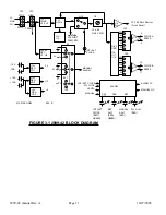
3.1 Block Diagram Discussion - 2099-42 (Figure 3.1) - The 10 MHz external reference signal goes to buffer
amplifier U15 and then to U1 which squares up the incoming 10 MHz signal. This reference signal then goes to
the synthesizer IC U2. U2 is programmed by controller U3 which provides data required for the synthesizer to
function. The VCXO U5 provides the other input signal into the synthesizer U2. This is controlled through a
switch consisting of U10 which determines whether the PLL is closed through loop amplifier U4 or if the
frequency of the VCXO is determined by the front panel potentiometer R20 which sets the VCXO frequency
when phase lock is broken or the external reference frequency has been removed. The output of U5, the VCXO
also goes through buffer U6 and Q2 to a front panel test point TP1 for monitoring this frequency. The
12.288 Mhz output of the VCXO also goes to divider U9, U11, and U12. The outputs of U11 and U12 provide
the clock signals at 64, 128, 256, 96, and 192 kHz. These signals go to jumpers JP4 and JP5 which are used to
select the desired output clock frequency. These signals go to RS422 driver U14 to provide the clock A and
clock B RS422 outputs.
The external 10 MHz reference frequency also goes to buffer amplifier U7 which drives peak detector
CR8 and then goes to op amp U8, the output of which provides a +5 signal if the 10 MHz signal is present and a
0 volt signal if not present. This logic signal goes to switch S1 which selects manual, internal, external, or
automatic mode. The output of S1 drives analog switch U10 through which the controls for the VCXO are
routed. The output of S1 also goes to the manual indication LED DS1 and U6, a buffer amplifier which drives
open collector output through Q1. The reference present signal out of U8 also goes to U13 which drives the
reference alarm LED DS3. The output of the switch also goes to U13 which drives the red/green
external/internal clock LED DS2. The lock detect output out of U2 goes to diode CR6 which detects the
incoming signal which is a non-DC signal if the loop is out of lock. Presence of this AC signal is detected by
U16 which drives DS4, the PLL alarm LED and also provides the PLL alarm signal which is diode OR'd with
the reference present signal to drive Q3, the FET, which enables the relay K1 which provides contact closures
indicating presence of a major alarm.
Regulators VR2 and VR1 p12 and -12 volts from the diode OR'd ±15V input and VR3 provides
+5V for the logic circuitry.
2099-42 manual Rev. A
Page 10
10/27/2005

