Copyright
©
2010
congatec
AG
QTOPm14
52/80
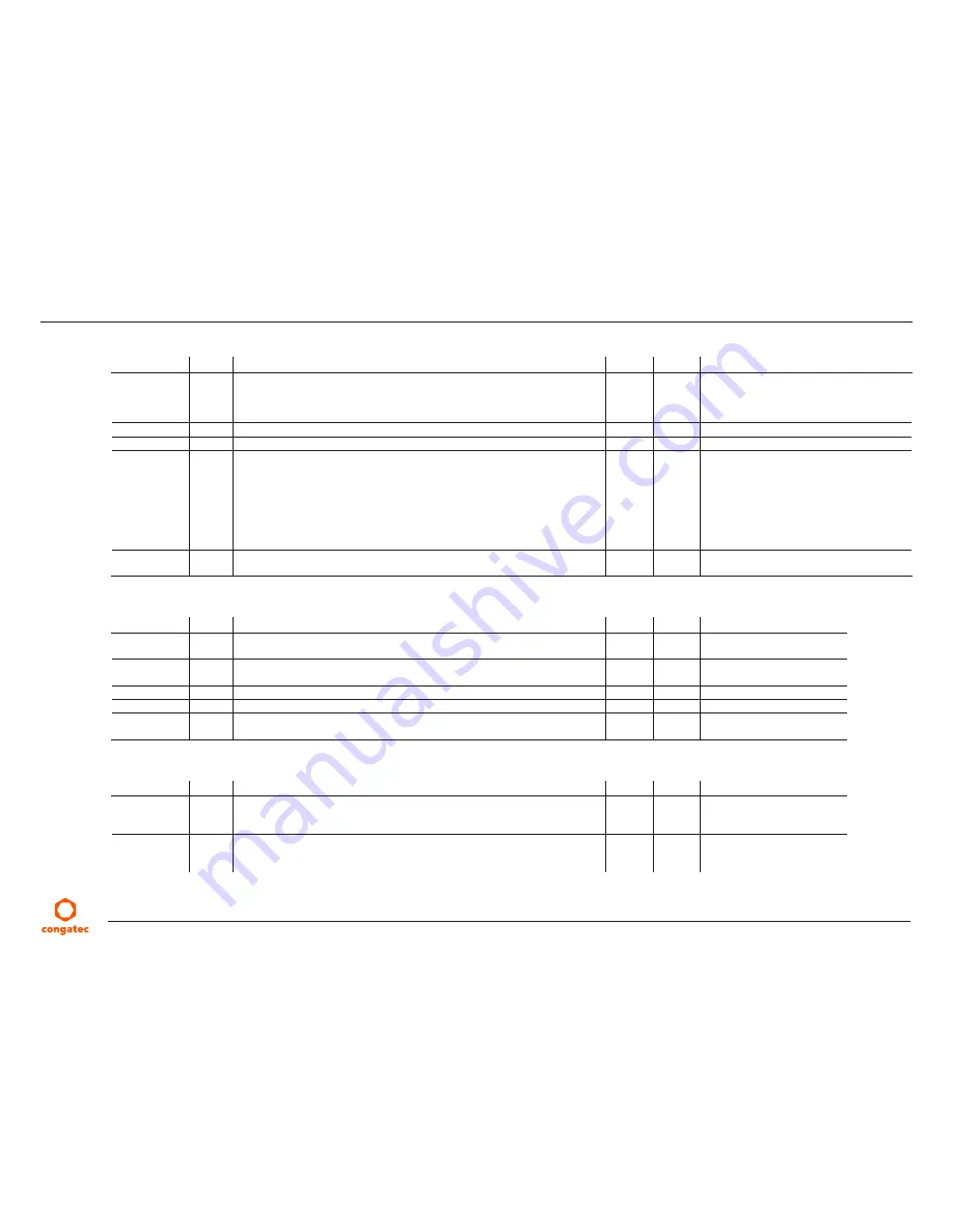
Table 23
LPC Signal Descriptions
Signal
Pin #
Description
I/O
PU/PD Comment
LPC_AD0
LPC_AD1
LPC_AD2
LPC_AD3
185
186
187
188
Multiplexed Command, Address and Data.
I/O 3.3V
LPC_FRAME#
190
LPC frame indicates the start of a new cycle or the termination of a broken cycle. O 3.3V
LPC_LDRQ#
192
LPC DMA request.
I 3.3V
Not Supported
LPC_CLK
189
LPC clock.
O 3.3V
The LPC clock output operates at 1/4th of
FSB frequency. By default, the LPC clock is
only active when LPC bus transfers occur.
Because of this behavior, LPC clock must be
routed directly to the bus device; they cannot
go through a clock buffer or other circuit
that could delay the signal going to the end
device.
SERIRQ
191
Serialized Interrupt.
I/O 3.3V PU 10k
3.3V
Table 24
SPI Interface Signal Descriptions
Signal
Pin #
Description
I/O
PU/PD Comment
SPI_MOSI
199
Master serial output/Slave serial input signal. SPI serial output data from Qseven
®
module to the SPI device.
O 3.3V
SPI_MISO
201
Master serial input/Slave serial output signal. SPI serial input data from the SPI
device to Qseven
®
module.
I 3.3V
SPI_SCK
203
SPI clock output.
O 3.3V
SPI_CS0#
200
SPI chip select 0 output.
O 3.3V
SPI_CS1#
202
SPI Chip Select 1 signal is used as the second chip select when two devices are
used. Do not use when only one SPI device is used.
O 3.3V
Not Supported
Table 25
CAN Bus Signal Descriptions
Signal
Pin #
Description
I/O
PU/PD Comment
CAN0_TX
129
CAN (Controller Area Network) TX output for CAN Bus channel 0. In order
to connect a CAN controller device to the Qseven
®
module’s CAN bus it is
necessary to add transceiver hardware to the carrier board.
O 3.3V
CAN0_RX
130
RX input for CAN Bus channel 0. In order to connect a CAN controller device to
the Qseven
®
module’s CAN bus it is necessary to add transceiver hardware to the
carrier board.
I 3.3V
PU 10k
3.3V


