background image

7.3  System and y-debugger  commands

Two MSDOS  and CP/M-86  system commands  are available,  depending on


the  application of  OS  control.

Command  concerning to hardware are  described here,  and  for other


commands  and  their details,  see MSDOS  User’s  Guide of  CP/M-86


User’s Guide.

y-debugger  commands  are  debugger  commands  designated  in  firmware.

7.3.1  MSDOS  system commands

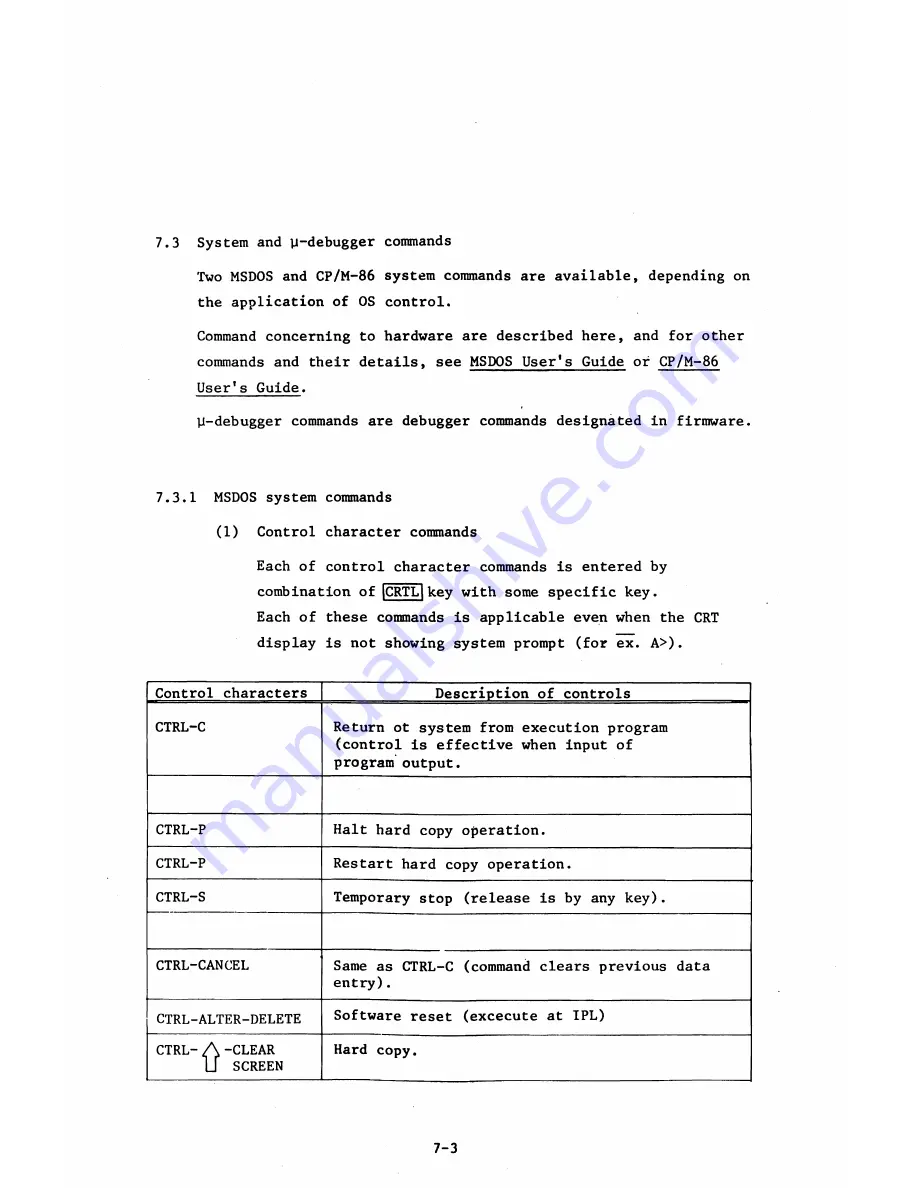
(1)  Control  character commands

Each of  control  character  commands  is  entered by


combination of |CRTLlkey with some  specific key.

Each of  these  commands  is  applicable even when  the  CRT


display  is not showing system prompt  (for ex.  A>).

Control  characters

Description of  controls

CTRL-C

Return ot  system from execution program


(control is  effective when  input of


program output.

CTRL-P

Halt hard  copy operation.

CTRL-P

Restart hard  copy  operation.

CTRL-S

Temporary stop  (release  is  by  any  key).

CTRL-CANCEL

Same  as  CTRL-C  (command  clears previous  data


entry).

CTRL-ALTER-DELETE

Software  reset  (excecute  at  IPL)

CTRL- A  -CLEAR


U   SCREEN

Hard  copy.

7-3

Summary of Contents for AS-100C

Page 1: ...Canon FIELD SERVICE MANUAL ...

Page 2: ...pter 2 Specifications Chapter 3 Disassembly Reassembly and Nomenclature of Each Section Chapter A Installation Chapter 5 Replacement and Ajustment of Units Chapter 6 Periodic Maintenance Chapter 7 Troubleshooting Chapter 8 Appendix ...

Page 3: ...ard memory 128KB 256KB or 384KB 2 RS 232C 2 expansion 3 RTC expansion 2 CRT CONT2 X 1 Gate array 2 Option B W display 1 Chip expansion VRAM 32KB 3 Additional functions of optional memory is for B W display 1 Partial high brightness 2 Partial blink 1 Memory chip expansion 128KB 2 RS232C on I O MOTHER 3 CENTRONICS interface 4 COMMUNICATION interface 5 POINTING DEVICE 1 Memory board expansion 128KB 2...

Page 4: ...FAN Below CRT Rear Cover FAN Below CRT Rear Cover B W display None None B W display None 1 Color display 1 None Color display 1 UNIT CRT UNIT B W Normal brightness UNIT CRT UNIT B W Normal brightness Partial high brightness Partial blink ...

Page 5: ...on This service manual is applicable only to the specified models as shown below Abbreviations of models are listed in Table 1 1 1 Model No f Sequential numbers Voltage No n 1 Fixed n 2 120V 3 230V A 2A0V 5 115V ...

Page 6: ...c r i p t i o n o f F u n c t i o n s 1 2 1 CPU 1 2 2 I O CONT I O Controller 1 2 3 DISPLAY CONT Display Controller 1 2 4 KEYBOARD 1 2 5 5 FDD 1 2 6 8 FDD 1 2 7 PRINTER 1 2 8 I O MOTHER option 1 2 9 RS232C option 1 2 10 CENTRONICS option 1 2 11 COMMUNICATION option 1 2 12 CURRENT LOOP option 1 2 13 5 HARD DISK option ...

Page 7: ...WING 5 FDD FDD BUS f62Kb MAX 4 DEVICES USER SELECTION APPLIABLE CONBINATION OF 5 FDD AND 8 FDD ARE FOLLOWING I I G T 1 5 3 I FDD 1 2 OPT4 OPT3 OPT2 RS232C O 0 O COMMUNICATION O CENTRONICS O CURRENT LOOP O o o H DISK I F O 3 2 I o l f II i __V__I I 5 FDDx2 1 rf 5 FDD 5 FDD 8 8 FDD 8 FDD 8 FDD It jp 4 1I Is I 9 I 1 II a I 1 8 FDDx2 3 i lO L 1 8 5t r HARD DISK POWER SUpPlf I i J APPLIABLE CONBIANTION...

Page 8: ...isk are incorporated KEYBOARD AS KEYBOARD ASCII A llll E21 0040 ASCII Key 10 key 5 FDD Minifloppy disk A 1300 E71 0050 2 sides double density double tracks mini drive x 2 File capacity 1 4MB max 8 FDD Floppy disk A 1330 E71 0061 2 sides double desntiy standard slim drive x 2 File capacity 2 5MB max PRINTER Dot impact printer A 1200 E71 0081 9 pin wire dot serial 80 characters 120CPS 480 dot image ...

Page 9: ... board A 1010 E71 0210 I O optional MOTHER board To A 1011 RS232C Serial data interface A 1500 E71 0150 RS 232C interface CENTRONICS Parallel data interface A 1502 E71 0190 CENTRONICS interface COMMUNICA TION Communication interface A 1503 E71 0180 Transmission 5 HARD DISK Hard disk A 1350 E71 0331 5 hard disk mini drive x 1 File capacity of hard disk 8 4MB Transfer rate of hard disk max 500KB H D...

Page 10: ...hic ISAM TZ Standard Level ISAM Extended Level Color Graphic Level I Table Handling Graph Level H F ile Handling Level m ON LINE Wordprocess1ng BSC 1 2 3 3780 3270 MCX2CPM F ile Converter from MCX CX 1 OS to tf M 86 VOLCOPY High Speed Media Copy FORMAT Media Formatter MS2CPM F ile Converter from MS DOS to CP M 86 SORT MERGE U t ilit y Standard Level Extended Level 5 Inch Hard Disk Support Standard...

Page 11: ...s a CPU To assure each model of good universality over programming both CP M 86 and MS DOS of a general use type are applied for operating system The CRT display B W or color is of a full graphic design It displays all images including characters with picture dots C N l O H fa 1 5 Functional Block Diagram ...

Page 12: ...ck 3 Timer check A Key check Clearing of VRAM in display controller Initialization of hardware for FDD controller OS loading from the system media into RAM by DMA controller I Operation of OS CP M 86 MS DOS Henceforth management under OS System memory map under the OS 00000H System memory 512KB 80000H 90000H FE000H FFFFFH Basic 256KB 00000H BIOS S y Z s y memory OS VRAM 32KB SUB SYSTEM i f l i f l...

Page 13: ...mory area appropriated for 8088 processor is divided into two as shown in Fig 1 2 3 One is the system memory area and the other is I O memory area This memory area division is performed automatically within the same address area of 20 bits 1 MB by a microprogram 00000H 0000H System memory area I O memory area 64 KB 1 MB FFFFH FFFFFH ROM RAM Hardware memory area for I O controller Example Hardware ...

Page 14: ...expandable by 128KB up to 512KB I O CONT See 1 2 2 Option involved in the CUP System memory RAM Up to 512KB max by expansion of each bord 128 256 384KB Real Time Clock RTC Data and time control It functions by backup of battery when power OFF 1 2 2 I O CONT I O CONT modifies the system bus into the I O bus in order to control the circuit of device option device and desplay controller which are con...

Page 15: ...tware timer for firmware of CPU Provides three different frequency pulse signals which varied by firmware of CPU I KEY INPUT Output to change tone of speaker output and a data transfer clock pulse to RS 232C of 1 Converts Key matrix code which is to be serially transferred from the keyboard and then to the parallel code Converted parallel code is directly transferred to CPU I SPEAKER AMP I T_RS232...

Page 16: ...32KB x 3 VRAM is accessable on a time sharing basis either the GDC or the CPU via the I O bus Picture structure of both black white and color display is as shown in Fig 2 4 color display only i 1 80x8 40 bit AN 80 characters x 25 lines Fig 1 2 4 For black white and color displays a pallet display system is employed and eight different patterns made from 1 or 3 VRAMs enhances display performance Fi...

Page 17: ...display Referring to Fig 1 2 5 dot timing is as in Table 1 2 1 Table 1 2 1 Bit output Selected pallet Output to display R G B 0 Pallet 0 No display Pallet 1 Normal display Option VRAM G included 1 0 Pallet 2 Partial high brightness display 1 1 Pallet 2 Partial normal brightness blink Color display Like the black white display depending on the contents of selected pallets six different chromatic si...

Page 18: ...ion 27 combinations of 3 colors are possible as indicated by the solid line Referring to Fig 1 2 5 eight different patterns are selected in advance on the pallets therefore eight colors be selected differently from the 27 colors Option in DISPLAY CONT VRAM Optional chip of 32 KB x 1 for B W display 1 2 A KEYBOARD I O CONT KEY BOARD KEY INPUT CLOCK DAT RESi ROM 1KB Key dataRAM 64B CPU 80A1 Key matr...

Page 19: ...onfirmation of key release when key code is same as D key data IB 8th bit is 0 are serially transferred n _ I Confirmation of key release when key code is same as 3 key data IB 8th bit is is l are _ serially transferred Key data are generated respectively when a key is pressed and released then serially transferred to key input circuit CPU converts key data into internal codes When key release tim...

Page 20: ...nterface circuit VFO circuit Power source Built in 1 2 7 PRINTER Refer to PRINTER TECHNICAL GUIDE 1 2 8 I O MOTHER option The I O MOTHER is for optional interface and devices to be connected to I O bus I O mother keeps a 96KB system memory area for optional use and a 3 port 0PT2 0PT3 0PT4 for optional interface addressed in I O memory area The following optional device and interface are connected ...

Page 21: ...PT3 1 0 0 1 1 1 0 0 _ OPT4 1 0 1 0 1 1 0 1 Note AO v A8 are address buses Optional port Option interface 0PT2 RS232C CENTRONICS CURRENT LOOP 0PT3 RS232C COMMUNICATION CURRENT LOOP 0PT4 RS232C H DISK I F CURRENT LOOP 1 2 9 RS232C option RS232C serial interface connected to I O MOTHER 1 2 10 CENTRONICS Option CENTRONICS interface connected to I O MOTHER 1 2 11 COMMUNICATION Option COMMUNICATION inte...

Page 22: ...consists of a M4863 hard disk a MDD220 and power supply unit M4863 connects to H DISK interface circuit which provides in MAIN UNIT through the disk controller built in M4863 MDD 220 connects to FDD CONT through 5 FDD interface circuit 1 16 ...

Page 23: ...Chapter 2 Specifications 2 1 MAIN UNIT 2 2 5 FDD 2 3 8 FDD 2 4 KEYBOARD 2 5 PRINTER 2 6 Option I n t e r f a c e 2 7 O p t i o n O t h e r s 2 8 General Specification ...

Page 24: ...bus Speaker output 16 bit processor 8088 Microprogram 4 MHz 8 types 8K bytes 1 Serial bus 36 KB S 2 Centronics bus 142 KB S 3 FDD bus 62 KB S 500 Hz to 4 KHz programmable Size 12 No of dots 640 horizontal dots x 400 vertical dots Character AN 80 characters x 25 lines Other functions Ruled line drawing in inter line space full graphic smooth scrolling Option B W VRAM 32KB x 1 can be added Additiona...

Page 25: ...ory 32 KB Options VRM set 128 256 384KB MEMORY BOARD RS 232C 1 RS 232C 2 interface Refer to 2 6 CENTRONICS COMMUNICATION interface Refer to 2 6 RTC set Refe r to 2 7 CURRENT LOOP interface HARD DISK interface Refer to 2 6 Power Source Input Output Effici ency Voltage Frequency Phase 5V 12V 12V Connector AC115V 10 AC120V 10 AC230V 10 AC240V 10 48 440 Hz Single phase 2 wire Max 8A OC provided Max 2 ...

Page 26: ...2 2 5 FDD Media Canon specified MDD 512DD 512B sector 2 3 ...

Page 27: ...8KB 1024B No of tracks 77 No of sectors 8 Recording density 6816 BPI Data transfer speed 500 Kb s Recording system MFM Access Time Seek time 3ms Settling time 15ms Latency time 83ms Error rate 10 12 B 10 6 SEEK Power source 24V 3 0A 5V 3 6A YD 180 1 drive speci fications henceforth In case of media given in format of 1024B sector Built in Media Canon specified MDD 256D 256B sector 2 4 ...

Page 28: ...7 4 i n s 4 5 8 5 angle adjust able T m 0 0 i l c c D c i p L 1 j aon T 1 T HOU Weight 2 2 kg Power con sumption Included in the CPU power consumption Type of keys See Fig 2 4 1 Data transfer speed 3 6 Kb S Fig 2 4 1 Keyboard 2 5 PRINTER Refer to PRINTER TECHNICAL GUIDE 2 5 ...

Page 29: ...al equipment 1 CENTRONICS Item Description Interface Conforms to interface produced by CENTRONICS Co standard Data format Parallel data Bit configuration 7 or 8 bits I communication e O H H u C c ü a o Synchronization mode SYN system start stop system Baud rate 300 600 1200 2400 4800 9600 MODEM synchronization Ht H c o 3 M Error control CRC check horizontal vertical parity 6 u g a o o Communicatio...

Page 30: ...ICURRENT LÖÖPl Available soon 2 7 ...

Page 31: ... sumption Included in CPU Transfer rate Conforms to keyboard IR T Cl Item Description Remark LSI used HD 146818 Real time clock RAM Accuracy 50 sec month Power supply 1 DC 5V 10 At operating 2 Min 3 0VDC Back up BATTERY More than 36 hours operation after the battery is fully recharged Recharging time 40 hours 2 8 ...

Page 32: ...rack Sector 1240 B sector No Sector in Track 9 sector track Cylinder 157 user area No of Track 960 Recording Density 7900 bPi Recording Method MFM Data Transmission Speed 625 KB sec MAX Avarage Access Time 75 m sec Disk Revolution 3600 v p m Start up 15 sec Error rate 10 12 b 10_12 SEEK Power 12 V 2 A MAX 4 0 A 5 V 1 Refer to mini floppy disk specification page 2 2 2 9 ...

Page 33: ...80 10 80 30 day No mist Vibration Below 0 25G Below 1G Shock Below 5G Power Supply AC115V AC120V AC230V AC240V 10 50 60 Hz Noise Resistance 1 Pulse peak 0 6KV 2 Pulse width 800ns 3 Repetitive frequency 50 Hz Insulation 1 Leak current Below 0 4m 2 Insulation resistance Below lOMfl under DC500V 3 Withstanding voltage 1 minute under AC100V Other 2 10 ...

Page 34: ...nclature of Each Section 3 1 MAIN UNIT 3 1 1 External view 3 1 2 Internal view 3 2 KEYBOARD 3 2 1 External view 3 2 2 Internal view 3 3 5 FDD 3 3 1 External view 3 3 2 Internal view 3 4 8 FDD 3 4 1 External view 3 4 2 Internal view 3 5 PRINTER ...

Page 35: ...nd color 3 1 1 External View Fig 3 1 1 Front View Fig 3 1 2 Rear View 1 A plate to cover 1 Remova 1 procedure of housing frame cover option interface connector Remove three retaining screws from 2 B plate to cover rear cover option interface connector 3 3C Plate to cover optional interface connector 3 1 ...

Page 36: ...NT P C B and fan internal cable from rear cover 5 Remove three grounding cables Fig 3 1 3 which are clamped to power supply unit then remove rear cover CPU I O CONT 4 Remove two retaining screws from the upper cover and slightly pull the upper cover toward yourself lifting it and removing it 3 2 ...

Page 37: ...3 1 2 Internal View Fuse 5A 1 pc CRT display I O MOTHER connector Speaker Brightness contro RESET key STOP key Core Key internal cable Fig 3 1 5 Fig 3 1 6 3 3 ...

Page 38: ...3 2 KEYBOARD 3 2 1 External View 1 Removal procedure of bottom cover I Bottom cover is removed first five retaining screws from bottom cover and loosening three retaining screws of rear cover 3 4 ...

Page 39: ...3 3 5 FDD 3 3 1 External View Housing plate Fig 3 3 1 Fig 3 3 2 3 5 ...

Page 40: ...g sheet 5 into MDD 220 2 Loosen two retaining screws Fig 3 3 3 at the left of front housing plate 5 Remove one retaining screw from rear cover and two retaining screws Fig 3 3 3 from bottom plate 3 3 2 Internal View Fig 3 3 4 shows the inside of 5 FDD with housing removed Fig 3 3 4 3 6 ...

Page 41: ...3 4 8 FDD 3 4 1 External View Housing Fig 3 4 1 Fig 3 4 2 3 7 ...

Page 42: ...ews Fig 3 4 2 from rear cover 3 Remove four retaining screws Fig 3 4 3 from bottom cover 4 Pull housing toward yourself while slightly lifting it Bottom p la te r e t a i n i n g screw Bottom plate retaining screw Fig 3 4 3 3 4 2 Internal View 8 F D D l F P c SFD signal cable SFD signal cable Fig 3 4 4 3 8 ...

Page 43: ...3 5 PRINTER Refer to PRINTER TECHNICAL GUIDE 3 9 ...

Page 44: ...nnections 4 2 4 Turning ON p o w e r s u p p l y b r i g h t n e s s a d j u s t m e n t a n d speaker output adjustment 4 2 5 Execution of test program and confirmation 4 3 Installation of Options 4 3 1 I O MOTHER E P C B 4 3 2 Optiona interface 4 3 3 V i d e o M e m o r y 4 3 4 O p t i o n M e m o r y B o a r d 4 3 5 Pointing Device ...

Page 45: ... MAX 25W X 8220A MAX 90W AP400 500 KSR MAX 85W Table 4 1 2 For 115V 120V 230V 240V j Model Wattages Model Wattages Model Wattsges Model Wattages M UNIT B W 125W M UNIT B W 175W M UNIT B W 175W M UNIT if B W 223W 4 5 FDD COLOR 1SOW 8 FDD COLOR 200W 5 8 FDD COLOR 200W 8M 8 FDD COLOR 250W Note At least three power receptacles are required Never connect the system directly to an AC line receptacle or ...

Page 46: ...ation 3 Cable connections 4 Turning on power supply brightness adjustment and speaker output adjustment 5 Execution of test program Refer to paragraph 4 3 for the method of installing options 4 2 1 Unpacking including confirmation of the component parts 1 Unpacking D MAIN UNIT BLACK WHITE COLOR Fig 4 2 1 4 2 ...

Page 47: ... 2 KEYBOARD 3 5 FDD 4 3 ...

Page 48: ... 8 FDD 4 4 ...

Page 49: ... E P C B and mounting place with a locking support SERIAL I F A 1500 RS232C P C B 25P mounting plates A and B OP M EM ORY A 1020 128K A 1021 256K A 1022 384K Expansion memory board and four retaining screws VEDEO RAM A 1004 Expansion video memory chip 16 COMMUN I F A 1503 SIO P C B PARALLEL I F A 1502 II CNT I F 2 P C B SERIAL I F A 1500 II RS 232C 2 P C B RS 232C 2 cable and four retaining screws...

Page 50: ... FDD 3 MAIN UNIT B W COLOR 5 FDD 8 FDD 4 MAIN UNIT B W COLOR 8 FDD 8 FDD Necessary to confirm and set the switches in the P C B according to each system configuration 1 Description of the switch bits in each P C B I CPU I O CONT P C B o SW1 Printed name Clock chip Provided OFF Not provided ON Unused Set at the OFF position Future use Future use rON 0 lOFF 1 Table 4 2 3 ...

Page 51: ...d Set to OFF position Unused Set to OFF position CRT ON B W lOFF White CRT ON 1 Picture OFF 2 Pictures Color JIS ASCII ON ASCII lOFF JIS Unused Set to OFF position Unused Set to OFF position DEBUGGER CONSOL ON Unused jOFF CRT KBD MAIN UNIT ON 0 OFF 1 For the significance of X see the description concerned Table A 2 4 4 7 ...

Page 52: ... 3 5 FDD I F P C B o SW1 Table 4 2 5 8 FDD l F P C B o SW1 Refer to paragraph 3 that the switches in respective P C B inside are present MDD 220 and YD 180 4 8 ...

Page 53: ...8 FDD C D 4 MAIN UNIT B W COLOR 8 FDD A B 8 FDD C D In each of above system configurations it is necessary to set swithces located in following P C B 1 8 FDD I F P C B C and D sides Set following switches of SW1 switch in 8 FDD I F P C B to specified positions No 5 OFF No 6 ON No 7 OFF No 8 ON The switches specified In each of P C B other than those above must go through only the confirmation for ...

Page 54: ...F Disk drive B MDD 220 Disk drive A MDD 220 Fig 4 2 9 These switches are set to the positions as specified in Table These switches are set to the positions as specified in Table Table 4 2 8 o SW3 1 2 3 4 5 6 At time of factory shipment ON OFF OFF ON ON OFF Table 4 2 9 These switches are set to the positions as specified in Table Note Disk drives A and B switches are set in same position 4 10 ...

Page 55: ...jumper plug and terminator Disk drive Terminator VFO timing Data transfer system Device select A C Provided Fig 4 2 12 Fig 4 2 13 Fig 4 2 14 B C Not provided Fig 4 2 15 Table 4 2 10 FD 0 0 SD Fig 4 2 12 VFO timing Fig 4 2 13 Data transfer system O c o a c 1 O o m r 0 o o m c m is 1 o o a l O 0 c 3 o o 0 s Fig 4 2 14 DEVICE SELECT A C Fig 4 2 15 DEVICE SELECT B D 4 11 ...

Page 56: ...and grounding cable The printer to be installed on MAIN UNIT is either DOT IMPACT PRINTER A 1200 or COLOR PRINTER A l210 1 Installation of 5 FDD FDD cable D Centronics cable D KEYBOARD cable 5 FDD power cable Printer power cable MAIN UNIT power cable Grounding cable Fig 4 2 16 2 Installation of 8 FDD FDD cable 2 Centronics cable 3 KEYBOARD cable 8 FDD power cable Printer power cable MAIN UNIT powe...

Page 57: ... cable 5 Centronics cable 3 KEYBOARD cable 4 5 FDD power cable D Printer power cable 6 MAIN UNIT power cable Grounding cable D 8 FDD power cable Fig 4 2 18 4 Installation of two 8 FDDs C D D D FDD cable Centronics cable KEYBOARD cable 8 FDD power cable Printer power cable MAIN UNIT power cable Grounding cable Fig 4 2 19 The following is the installation procedure 4 13 ...

Page 58: ... 5 FDD I F P C B See paragraph 4 2 3 Then mount 5 FDD onn5 FDD boss of properly with 5 FDD mounting holes of MAIN UNIT T Connect keyboard cable centronics and FDD cable to respective connectors of MAIN UNIT as in Fig 4 2 20 0 Clamp both centronics cable and FDD cable with connector lock pins 5 Connect 5 FDD power cable to its corresponding connector of MAIN UNIT and connect MAIN UNIT power cable t...

Page 59: ...en connect each power supply cable to its AC plug sdcket Attach grounding cable of printer to lower side öf printer power supply cable and clamp it to grounding cable connection position of MAIN UNIT together with grounding cable of 5n FDD 4 15 ...

Page 60: ...to respective conneectors of MAIN UNIT as in Fig 4 2 21 Clamp both centronics cable and 8 FDD cable with connector lock pinsc 3 Connect main unit power supply cable and 8 FDD power supply cable to their corresponding receptacle 4 After checking that printer power switch set to OFF connect printer power supply cable to AC power receptacle 5 Clamp printer grounding cable to the part below printer po...

Page 61: ...DD expansion cable for FDD con nector 1 as in Fig A 2 18 Note Attach device seals C and D to positions marked A and B on the front of 8 FDD MAIN UNIT 8 FDD 8 FDD Refer to installation of MAIN UNIT 8 FDD Fig 4 2 23 Note Attach device seals C and D to positions marked A and B on the front of 8 FDD Refer to a of Fig 4 2 23 4 17 ...

Page 62: ... system media to 5 FDD Turn on power supply to MAIN UNIT 2 Turning off power supply Turn off printer power supply Turn off MAIN UNIT power supply When 8 FDD is to be connected to MAIN UNIT 1 Turn on power supply Turn on power supply to printer Turn on power supply to 8 FDD Set system media to 8 FDD Turn on power supply to MAIN UNIT 2 Turning off power supply Turn off printer power supply Turn off ...

Page 63: ...put adjustment Remove the rear cover of MAIN UNIT see paragraph 3 1 of Chapter 3 Remove system media after OS is loaded in then adjust speaker tone with entering keys by the speaker output control knob on I O CONT P C B as In Fig 3 1 4 4 2 5 Execution of test program and confirmation Refer to TEST PROGRAM OPERATIONAL MANUAL separately provided for details regarding the execution of a test program ...

Page 64: ...ver and upper cover See paragraph 3 1 2 Referring to paragraph 5 2 2 of Chapter 5 pull out power supply unit half its entire depth and disconnect each cable For 115 120V Fig 4 3 1 T Install the I O MOTHER mounting plate using three retaining screws as shown in Fig 4 3 1 4 20 ...

Page 65: ...OTHER DC cable of I 0 M0THER E f C B to No 4 connector Fig 5 2 4 of switching regulator 6 Lock grounding cable from I O MOTHER E P C B to chassis of power supply unit as in Fig 5 2 2 Rass I O MOTHER internal cable between MOTHERBOARD rack and CRT unit Connect I O MOTHER internal cable to I O MOTHER connector Fig 3 1 5 on M0THERV0ARD with alignment A mark 4 21 ...

Page 66: ...of RS232C P C B is different according to the location The rear side of each 25P mounting plate has an A mark No 2 and 3 marked on rear panel Make sure whether or not 25P mount ing plate A alphanumeric mark EA4 0079 is fitted to RS232C P C B No 4 marked on Exchange 25P mounting plate A to B rear panel D Remove both rear and upper covers See paragraph 3 1 of Chapter 3 5 Pull out power supply unit h...

Page 67: ...lamped to power supply unit with two retaining screws 4 Referring to paragraph 4 3 1 of Chapter 4 install I O MOTHER mounting plate and I O MOTHER E P C B As in Fig 4 3 4 fit RS232C P C B tö I O MOTHER E E C B Fig 4 3 4 4 23 ...

Page 68: ... 6 Fix power supply unit reinforcement mount in position and clamp grounding cable from l 0 M0THER E P C B to chassis of power supply unit see Fig 5 2 2 4 24 ...

Page 69: ... CONT P C B from MAIN UNIT by reference to 5 2 1 Fig 4 3 6 CPU I O CONT P C B 0 As in Fig 4 3 6 connect RS232C 2 P C B to CPU I O CONT P C B while paying attention to the connector Fix it using two screws on soldered side of CPU l O CONT P C B optional interface Spacer connector Fig 4 3 7 4 As in Fig 4 3 7 remove the palte to cover option interface connector 4 25 ...

Page 70: ...RS 232C 2 cable Fig 4 3 8 As in Fig 4 3 8 connect RS 232C 2 cable to RS 232C 2 P C B RS 232C 2 port connector Fig 4 3 9 As in Fig 4 3 9 fix connector with 2 screws 4 26 ...

Page 71: ... ready for sending CB 6 DSR Data Set Ready AS 100 READY c c 7 SG Signal Ground ab 8 DCD Received Line Signal Detector Carrier detector CF 20 TRDY Data terminal Ready DEVICE READY CD Note Other pins are none connector 2 Connections AS 100 DEVICE FG TOT KXÖ l2v RTS I CTS f l O K 1 t DSR 12V SG T U CD flOK i I TRDY 1 1 2 2 3 3 4 4 5 5 6 6 7 7 8 8 20 20 FG TXB RXI5 RTS CTS DSR SG DCD TRDY Fig 4 3 6 Co...

Page 72: ...interface SIO P C B For SIO P C B number 3 marked on the rear panel is only connectable Connection method is the same as for RS232C P C B 4 SIO PCB SWITCH SW Printed name KH 2 G 3 F 4 E 5 D 6 C 7 B 8 A At the time of factory shipment OFF OFF OFF OFF OFF ON ON ON V Setting by user s software Synchro Asynchro nous nous ON OFF OFF ON Selectable each bit by software ON OFF OFF ON 4 28 ...

Page 73: ... are required to be switched 1 Remove the rear and upper covers Refer to 3 1 in Chapter 3 2 Remove CRT CONT2 B W P C B from MAIN UNIT by Option video memory area 32KB with socket G picture Fig 4 3 11 5 Expansion area of option video memory is provided with socket for 16 additional video memory chips 32KB Note Pay attention direction of each video memory chip prior to expansion ...

Page 74: ...d in Fig 4 3 11 as in Fig 4 3 12 JP circuit 2 o i l a section 2 o 1 a section Fig 4 3 12 Switch JP circuit from screen 1 to screen 2 Re solder JP circuit screen 1 on screen 2 Remove CPU I O CONT P C B from MAIN UNIT and set SW2 No 5 located on CPU I O CONT P C B to OFF Refer to 1 2 2 of Chapter 1 4 30 ...

Page 75: ... memory board ex pansion RS 232C 2 P C B expansion D RTC expansion Fig 4 3 12 CPU I O CONT P C B Remove rear and upper covers See paragraph 3 1 of Chapter 3 Remove CPU I O CONT P C B from MAIN UNIT by referring to 5 2 2 in Chapter 5 As in Fig 4 3 13 attach memory board to CPU I O CONT P C B with care in connecting connector Attach it with 4 screws on soldered side of CPU I O CONT P C B 4 31 ...

Page 76: ...Fig 4 3 13 4 3 5 Pointing Device Connect pointing device connector to its position on KEYBOARD See Fig 3 1 7 4 32 ...

Page 77: ...Unit configuration 5 2 HAIN UNIT 5 2 1 P C B 5 2 2 Power supply unit 5 2 3 CRT unit 5 2 4 Fuse replacement 5 3 KEYBOARD 5 3 1 KEYBOARD 5 3 2 Key top 5 4 5 FDD 5 4 1 MDD 220 5 4 2 5 FDD I F 5 5 8 FDD 5 5 1 YD 180 5 5 2 8 FDD I F 5 5 3 Power supply unit ...

Page 78: ...Units and Adjustment after Replacement Prior to replacing each units turn off power switch and unplug power cord from receptacle 5 1 Unit configuration and general assembly Refer to APPENDIX 5 2 MAIN UNIT 5 2 1 P C B Fig 5 2 1 ...

Page 79: ...ee paragraph 4 2 2 connect it in reverse order of above steps CONT 2 B W P C B First remove rear and upper covers see paragraph 3 1 Then disconnect CRT internal cable from CRT C0NT2 B W P C B Disconnect the grounding cables which are extending from individual P C Bs from the chassis of the power supply unit Remove CRT C0NT2 B W P C B from MAIN UNIT Connect spare CRT C0NT2 B W P C B in reverse orde...

Page 80: ... 2 CRT C0NT2 C T Remove rear and upper covers see paragraph 3 1 Then disconnect CRT internal cable from CRT unit 2 4 Same as for B W display Adjustment Test program check of operation 5 3 ...

Page 81: ...d upper covers see paragraph 3 1 1 of Chapter 3 2 Disconnect FDD internal cable from CPU I O CONT P C B 3 Disconnect grounding cables which are attached to individual P C Bs power supply unit and MOTHERBOARD RACK 4 Remove two retaining screws from power supply unit Fig 5 2 3 shows location of these retaining screws Retaining screw Power supply unit ...

Page 82: ... T Pull out power supply unit half its depth as in Fig 5 2 4 Then disconnect 5 FDD internal cable arid MOTHERBOARD DC cable from SWITCHING REGULATOR Fig 5 2 4 5 5 ...

Page 83: ...NG REGULATOR T Remove four retaining screws of SWITCHING REGULATOR to remove it Fig 5 2 5 Retaining screw Retaining screw AC Input cable For 230 240V Fig 5 2 5 8 Mount replaced SWITCHING REGULATOR in position and connect both AC input cable and grounding cable to SWITCHING REGULATOR and 5 FDD connector to red CN5 5 6 ...

Page 84: ...lated screw driver since high voltage are applied to heat sink and collector of transistors having caution labe Connectors Connector Mo Pin No Voltage 5 FDD internal power supply connector CN5 1 12V 2 GND 3 GND 4 5V I O MOTHER power supply connector CN4 1 12V 2 12V 3 GND 4 5V MOTHERBOARD power supply connector CN3 1 12V 2 12V 3 GND 4 5V Table 5 2 1 5 7 ...

Page 85: ...onnect brightness control VR cable and CRT power supply cable from CRT unit and CRT internal cable from CRT CONT 2 B W P C B 3 As shown in Fig 5 2 7 mark set position of CRT unit 4 Remove five retaining screws Fig 5 2 7 of CRT Unit and remove it from MAIN UNIT Mark the set position Fig 5 2 7 5 8 ...

Page 86: ... to marked set position 8 Connect disconnected cables Color display Remove both rear and upper covers as in paragraph 3 1 of chapter 3 Disconnect brightness control VR CRT internal cable and CRT power supply cables from CRT unit in Fig 5 2 8 C R T i n t e r n a l c a b l e Brightness control VR cable CRT power supply cable Shield p l a t e CRT CONT C P C B Mark the set position Fig 5 2 8 5 9 ...

Page 87: ...take out the fan cable Remove CRT unit from MAIN UNIT then remove the shield plate from CRT unit by two retaining screws Mount spare CRT unit to MAIN UNIT and tighten retaining screws while aligning it to the marked set position shield plate to spare CRT unit T Connect all disconnected cables Adjustment Same for B W and COLOR Confirm the operation with a test program 5 10 ...

Page 88: ...5 2 4 Fuse replacement 1 Keyboard fuse on MOTHERBOARD T Remove both rear and upper covers see paragraph 3 2 2 Replace fuse shown in Fig 5 2 9 on MOTHERBOARD Fuse Fan internal cable Fig 5 2 9 5 11 ...

Page 89: ... FDD fuse l Remove both rear and upper covers see paragraph 3 2 I Pull out power supply unit about half its depth Refer to 5 2 2 T Replace two 5A fuses as in Fig 5 2 10 Fuse Fig 5 2 10 For 120 230 240V 5 12 ...

Page 90: ...should be taken not to accidentally cut pointing device cable inside keyboard in removal 5 3 2 KEY TOP l Remove key top requiring replacing as shown in Fig 5 2 11 Fgi 5 2 11 D Apply adhesive to rear side of key top and set it on its cor responding key stem firmly pressing key top against stem 5 13 ...

Page 91: ...o MDD 220 J Remove housing plate see 1 of paragraph 3 3 1 3 Disconnect MFDD signal cable and MFDD DC cable from each MDD 220 Remove four retaining screws in Fig 5 4 1 from mounting plate 5 Remove MFDD retaining screws of defective mini floppy disk drive A or B to remove it from its mounting plate 5 14 ...

Page 92: ...eck set position of DIP switch of replacing mini floppy disk drive see 3 or paragraph 4 2 2 mount mini floppy disk drive according to dismounting reverse procedure 2 Adjustment Check the operation a test program 5 15 ...

Page 93: ...nding cable from 5 FDD I F P C B 4 Remove five retaining screws from 5 FDD I F 3 Remove 5 FDD power cable clamp from two retaining screws from chassis of 5 FDD I F P C B 6 After confirming set positions of 5 FDD I F P C B switches see 2 of paragraph 4 2 2 mount the replaced 5 FDD I F P C B according to dismount re verse procedure 2 Adjustment Check the operation with a test program 5 16 ...

Page 94: ...om tie band 4 Disconnect SFD signal cable and DC cable from 8 FDD I F PCB I Disconnect DC cable from YD 180 and also fan DC cable 6 Remove six retaining screws specified in Fig 5 5 1 Floppy disk drive B YD 180 Floppy disk drive A YD 180 Retaining screws 2 Disconnect SFDD signal cable from YD 180 8 Remove six retaining screws of floppy disk drive mounting plate A 5 17 ...

Page 95: ...signal cable Floppy disk drive mounting plate A Retaining screw of floppy disk drive mounting plate Fig 5 5 2 G Remove defective YD 180 from floppy disk drive mounting plate B Floppy disk drive B YD 180 5 18 ...

Page 96: ... After confirming set positions of replacing YD 180 switches 3 of paragraph 4 2 2 mount YD 180 in removal reverse procedure 2 Adjustment Confirm the operation with a test program 5 19 ...

Page 97: ... signal cable and DC cable from 8 FDD I F P C B Disconnect SFDD cable from YD 180 Remove four locking support from 8 FDD I F P C B After confirming set positions of replacing 8 FDD I F P C B switches see paragraph 4 2 2 mount 8 FDD I F P C B according to opposite removal procedure 2 Adjustment Confirm the operation with a test program 5 20 ...

Page 98: ...5 5 3 Power supply unit 5 5 1 Referring to 5 6 of paragraph 5 5 1 1 remove power supply unit Fig 5 5 5 5 21 ...

Page 99: ... supply unit 1 Disconnect all cables from power supply unit 2 Remove four retaining screws from rear side of base plate to remove power supply unit 1 Mount replacing power supply unit in the reverse way to the removal 5 22 ...

Page 100: ...8 FDD Fuse 1 Replace two 5A fuses 8 FDD as In Fig 5 5 7 5 23 ...

Page 101: ... Red 24V YD 180 x 2 2 Blue GND 3 Yellow 5V 4 Black GND 6 Brown GND P C B DC cable 1 Yellow 5V 8 FDD l F P C B 2 Black GND FAN DC cable 1 Blue GND FAN 2 Red 24V Power supply unit For 115V Power supply unit Rcc p acle Powtr witch Hoiie f ilt e r For 120 230 240V Fig 5 5 8 5 24 ...

Page 102: ...ADJUSTMENT Adjust the VR101 with an insulated screw driver so that 5V may be obtained at the 5V terminal of the power supply 5 25 ...

Page 103: ...Chapter 6 Periodical Maintenance 6 1 5 FDD 6 1 1 Periodical 6 1 2 Periodical 6 2 8 FDD 6 2 1 Periodical 6 2 2 Periodical maintenance items maintenance maintenance maintenance 6 3 PRINTER ...

Page 104: ...TE 5 2 CLEANING DISKETTE 8 Periodical maintenance includes cleaning MAIN UNIT and other devices 6 1 5 FDD MDD 220 6 1 1 Periodical maintenance items 1 Cleaning head Yearly 6 1 2 Periodical maintenance procedure With CLEANING DISKETTE 5 clean head of 5 FDD for 5 seconds while running TRK ADJ test program For details regarding TRK ADJ test program refer to TEST PROGRAM OPERATIONAL MANUAL provided se...

Page 105: ...dical maintenance procedure With CLEANING DISDETTE 8 clean head of 8 FDD for while running TRK ADJ test program For details regarding TRK ADJ test program refer to PROGRAM OPERATIONAL MANUAL provided separately 6 3 PRINTER r Refer to certain printer TECHNICAL GUIDE 1 minute the TEST 6 2 ...

Page 106: ... 7 Troubleshooting 7 1 At System Up 7 1 1 Error message 1 7 2 OS control error 7 3 System and y debugger commands 7 3 1 MSDOS system command 7 3 2 CP M 86 system command 7 4 DCOPY media copy program operation ...

Page 107: ...Chapter 7 Troubleshooting 7 1 At System Up 7 1 ...

Page 108: ... B Optional memory P C B 2 ERR CODE XX L Error code No Error code No Cause Remedy 02 ROM check sum error Replace ROM Replace CPU E P C B 03 PTM 6840 error Replace CPU E P C B 04 Key circuit error Replace I O CONT P C B Replace KEYBOARD Table 7 1 1 7 2 OS control error For error correction refer ot CP M Users Guide or MSDOS Users1 Guide After troubleshooting always apply a test program to the syste...

Page 109: ...ach of control character commands is entered by combination of CRTLlkey with some specific key Each of these commands is applicable even when the CRT display is not showing system prompt for ex A Control characters Description of controls CTRL C Return ot system from execution program control is effective when input of program output CTRL P Halt hard copy operation CTRL P Restart hard copy operati...

Page 110: ...AME EX DEVICE FILE NAME EX can be omitted Up to 3 alphanumeric characters 8 alphanumeric characters starting with an alphabetical character Given with one of alphabetical characters from A to D Current device name For file name and EX wild card and character conversion symbol are avaukable Command entry is terminated by pressing J key or ENTER key 2nd file name Comment BAT Batch file COM Command f...

Page 111: ...r 1st parameter unmatches current device Copy onto current device Command ends with message 0 File s Copied at error File Delete DEL 1st parameter 1st parameter file is deleted Directory Display DIR i j1st parameter 1st parameter is omissible Directory of 1st parameter file is desplayed When 1st parameter is omitted directory for all files is displayed File Rename REN 1st parameter 2nd parameter N...

Page 112: ...required DATE Current date is MM DD YYYY Enter a new date Current date display and registration of new date When there is no reregistration only enter feNTRYl kev For a misinput INVALID DATE is displayed arid requests re entry Time Entry Media must be set as required TIME Current time is HH MM SS CC Enter a new time Current time display and registration of new time When there is no reregistration ...

Page 113: ...FORMAT Formatter FORMAT i j 1st parameter Initialize media of 1st parameter device 1st parameter is only device name 5 floppy disk 512 bytes sector 8 floppy disk 1024 bytes sector 7 7 ...

Page 114: ...command is input once more it stops echoing the via console commands to the printer This command is effective only when the printer is connected to the computer system CTRL R Current command typed in again CTRL R command is serviceable after pressing RUN or DEL key CTRL S Temporarily stops output of list into console however Same command is input once more the output is resumed Console list CTRL U...

Page 115: ...n be omitted File name Device name Can be omitted Up to 3 alpha numeric characters 8 alphanumeric characters beginning with a certain alphabet ical character Given with one of the alphabetical characters from A to D Current device name For file name and EX the wild card and the character conversion symbol n n are available Command entry ends by pressing or ENTER key ENTERl key 2nd file names Comme...

Page 116: ...YS file is not displayed System Directory Display DIRS i 1st parameter DIRS is the same as DIR except for SYS file display File Erase ERA 1st parameter 1st parameter file is deleted Enter Y or N while ALL Y N is displayed File Rename REN 1st parameter 2nd parameter 1st parameter file name is renamed in 2nd parameter file name Note that designation of 1st parameter device name must be the same as 2...

Page 117: ... COPY DISK Copy Disk COPY DISK Entire contents of one floppy disk are copied onto another floppy disk Enter following parameters after entering this command Enter Source Disk Drive A D Destination Disk Drive A D Is this what you want to do Y N Copy another disk Y N PIP Peripheral Interchange Program PIP I 1st parameter Gn 2nd parameter n of Gn is a user number Contents of 2nd parameter file are co...

Page 118: ...Attribute of file is displayed as follows When SIZE is omitted the file size is not displayed File size No of records File capacity FCB num er File Control Block Attribute File name STAT 1st parameter RO Read only RW Read Write 1 These two cannot be specified at the same time SYS System access DIR Directory access These two cannot be specified at the same time Specify attribute of file No omission...

Page 119: ...EC P Current date and time display and exchange them TIME SPEC is designated in format of MM DD YY HH MM SS With P parameter the date and time are displayed con tinuously display stops by entering any key FORMAT Formatter FORMAT j 1st parameter Media of 1st parameter device is initialized 1st parameter is only device name 5 floppy disk 512 bytes sector 8 floppy disk 1024 bytes sector 7 13 ...

Page 120: ...mands and their meanings Key operations See abbreviations B Boot b n d cr D Display Memory D W ADDR ADDR2 CR G Go G CS IP OLD ADDR BRK CR 1 Port Input I W P0RT CR N Single Step N CS IP 0LD ADDR CR 0 Port Output 0 W P0RT NEW CR R Read Hex File R BIAS CR S Substitute Memory S W ADDR OLD t NEW CR X Examine Modify Register X CR X REG OLD NEW CR Table 7 3 5 Any of alphabetical characters within can be ...

Page 121: ...signates address both segment and offset When an omission is made from specified segment contents of CS are specified The specification with numeric value in hexa decimal notation of four digits The name REG register is specified for a numeric value Example SP 1234 Offset Segment hexadecimal or register name ADDR2 For 2nd address with value of segment given with a ADDR therefore the designation is...

Page 122: ... is waiting for command entry On the other hand if comma key is entered the same command will be executed at succeeding address The succeeding address remarked here signifies the following Current address 1 however I and 0 commands are excluded in the case of the byte access command Current address 4 2 in the case of the word access command Current address 4 number of bytes of the executed command...

Page 123: ...he hexadecimal and with two or four digits depending on the command PORT Designated port address in hexadecimal with four digits REG Each register of 8088 is indicated with two alphabetical characters as in the TAble below Register Name Abbreviation Accumulator AX Base BX Count CX Data DX Stack Pointer SP Base Pointer BP Source Index SI Destination Index DI Code Segment CS Data Segment DS Stack Se...

Page 124: ...igits following 0 Then CRT display shows for command entry Initial display of each content is not always given on the left side or the display area of CRT screen COMMANDS B Boot B N D CR Initial boot is performed with the floppy disk drive A N is fixed to 0 If D has been designated a debugger returns into initial boot D Display Memory D W ADDR ADDR2 CR Contents of respective addresses from ADDR to...

Page 125: ...turns to command I Port Input I W PORT CR When contents of designated port are displayed then enter CR When comma is entered contents of the same port is displayed at a time difference of same displayed port N Single Step N CS IPXOLD ADDR CR Contents of designated CS and IP are displayed in hexadecimal and with four digits Enter CR to execute single step To change the address of the program execut...

Page 126: ...address ADDR are displayed To examine the contents enter CR and change the contents enter NEW before CR entry Execute read after write check X Examine Modify Register X CR X REG OLD NEW CR When X CR is only designated name and contents of each register are displayed If REG is entered contents of a designated register is displayed To modify the register contents enter CR To modify register contents...

Page 127: ...ric value of some digits is greater than specified particular digits at the head part of numeric are cut off with no error message displayed Once an misinput happens no correction step is possible ex cept to intentionally make an error For example Enter misinput 3 then error message for command re entry appears Entry is only for alphanumeric ...

Page 128: ...7 4 D COPY media copy program operation Execute program D COPY to copy a test program For details of D COPY operation refer to TEST PROGRAM OPERATIONAL MANUAL 7 22 ...

Page 129: ...Chapter 8 Appendix 8 1 Unit Configuration and General Wiring ...

Page 130: ...8 1 Unit Configurations and General Wiring 8 1 POWER SWITCH ...

Page 131: ...r r Nn H YELLOW P ia N o W ire s color 4 Y E L L O W 5 V 3 B L A C K G N D 2 B R O W N G N D 1 O R A N G E M 2 V RS232C 2 P C B OPTION N o N o W in o o tw 4 v T i r n w t J Y 3 B J T f fO N D V 2 O R A N G E 1 M 1 Y 1 R O W H V ____ Mark i s s o ld e r in g co n n e ctio n 2 i s fo r 115V and 120V i s fo r 120V POWER SWITCH ...

Page 132: ... W ire s c olo r 4 Y E L L O W C 5 V 3 B L A C K G N D 2 B R O W N G N D 1 O R A N G E 1 2 V R S 2 3 2 C 2 P C B OPTION Pin N o W ire s color 1 O R A N G E 2 O R A N G E Pin N o W in s color 4 Y E L L O W J V 3 B L A C K G N D 2 O R A N G E 2 V 1 B R O W N I 2 V in N o W in s color 1 B R O W N 3 B LU E Mark is Soldering Connection POWER SWITCH ...

Page 133: ...A N C E t l 2 V 1 B R O W N I 2 V Pin N o W ir ookn V B R O W N 3 B L U E KEY C A BLUE 5 V B ORANGE C GREEN t i n n D _ B s n w N E GRAY renn F RED G BLACK r Nni H YELLOW Pin N o W ire color 4 Y E L L O W J V 3 B L A C K G N D ___ 2 _ j B R O W N G N D 1 O R A N G E 1 Z V RS232C 2 P C B OPTION 1 Mark is Soldering Connection P O W E R S W I T C H ...

Page 134: ...Pin No W in color 2 G REEN JV 1 R ED GN D 3 W H ITE G N D 4 BLA C K 12V Pin No W ir color 1 O RAN GE 12V 2 B LU E G N D 3 BLA C K G N D 4 YELLO W SV Fig 8 1 5 5 FDD For 115 120 230 240V 8 5 ...

Page 135: ...Fig 8 1 6 8 FDD For 115 120 230 240V POWER SWITCH ...

Page 136: ...CANON INC COPYRIGHT g 198 BY CANON INC Printed in Japan Feb 1983 E Y 8 6 0 7 2 2 2 2 ...

Reviews: