III-2
3.2
MAIN PCB
3.2.1
Main PCB Block Diagram
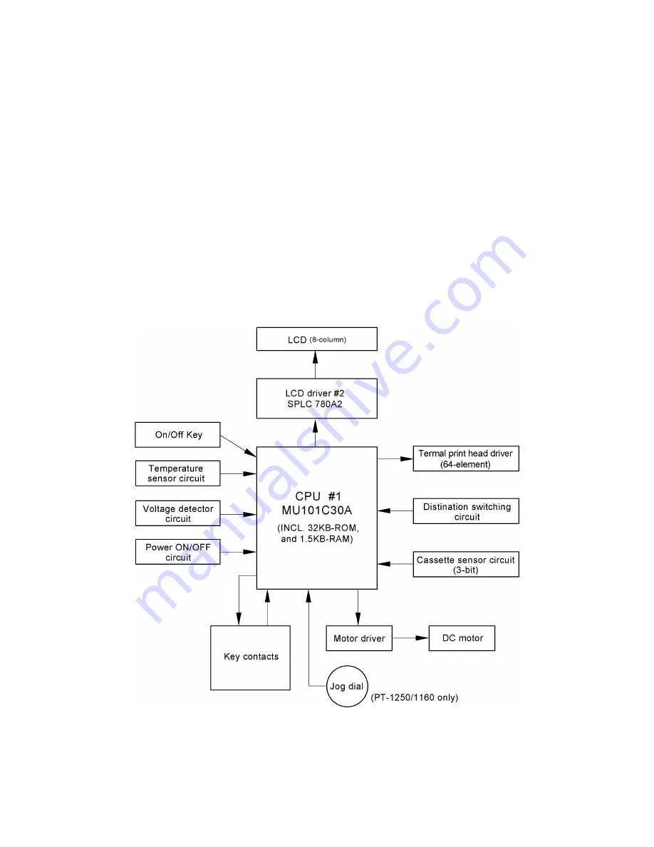
Fig. 3.2-1 shows the Main PCB block diagram. The PCB consists of the following:
(1)
CPU (including a ROM, RAM, and LCD control)
(2)
Key contacts matrix, solder points (specification switching-over circuit) and jog dial (PT-
1250/1160 only).
(3)
Power On/Off circuit and power saving circuit
(4)
Motor control circuit
(5)
Thermal head drive circuit
(6)
Voltage detection circuit and temperature sensor circuit
(7)
Oscillation circuit
(8)
Reset circuit
(9)
Power supply circuit
(10)
Cassette sensor circuit
Fig. 3.2-1 Main PCB Block Diagram
Summary of Contents for P-touch PT-1100
Page 2: ...SERVICE MANUAL MODEL PT 1100 1130 1170 1180 11Q PT 1250 1160 ST 1150 Heavy Duty LabelerTM ...
Page 5: ...CHAPTER I SPECIFICATIONS ...
Page 9: ...I 3 Fig 1 1 2 Key Arrangement 1 ...
Page 10: ...I 4 Fig 1 1 2 Key Arrangement 2 ...
Page 11: ...I 5 Fig 1 1 2 Key Arrangement 3 ...
Page 13: ...CHAPTER II MECHANISMS ...
Page 50: ...35 II 2 3 4 Troubleshooting Flows 1 Tape feeding failure ...
Page 51: ...36 II ...
Page 52: ...37 II 2 Printing failure ...
Page 53: ...38 II ...
Page 54: ...39 II 3 Powering failure Nothing appears on the LCD ...
Page 55: ...40 II 4 No key entry possible ...
Page 56: ...CHAPTER III ELECTRONICS ...
Page 75: ...III 17 3 3 3 Troubleshooting Flows 1 Tape feeding failure 2 Printing failure ...
Page 76: ...III 18 3 Powering failure Nothing appears on the LCD ...
Page 77: ...III 19 4 Abnormal LCD indication ...
Page 78: ...III 20 5 No key entry possible 6 Tape cassette type not identified ...
Page 80: ......
Page 81: ......
Page 82: ......


