background image

IPC@CHIP SC2x3 

Hardware Manual V1.02 [01.03.09]  


©2000-2009 BECK IPC GmbH 


Page 30


6.2.3  I²C 

The I²C bus is a popular serial, two-wire interface used in many systems because of its low overhead. Capable 

of 100 kHz operation, each device connected to the bus is software addressable by a unique address, with a 

simple master/slave protocol. 


The I²C bus consists of two wires, serial data (SDA), and a serial clock (SCL), which carry information between 

the  devices  connected  to  the  bus.  This  two-wire  interface  minimizes  interconnections,  so  integrated  circuits 

have fewer pins, and the number of traces required on printed circuit boards is reduced.  


The number of devices connected to the same bus is limited only by a maximum bus capacitance of 400 pF. 

Both  the  SDA  and  SCL  lines  are  bidirectional,  connected  to  a  positive  supply  voltage  via  a  2.2k   pull-up 

resistor. When  the bus  is  free,  both  lines  are  HIGH.  The output stages  of  devices  connected  to  the  bus  must 

have an open-drain or open-collector to perform the wired-AND function. 


Each device on the bus has a unique address and can operate as either a transmitter or receiver. In addition, 

devices can also be configured as masters or slaves. 


A master is the device that initiates a data transfer on the bus and generates the clock signals to permit 

that transfer. 


Any other device that is being addressed is considered a slave. 


The I²C protocol defines an arbitration procedure to ensure that if more than one master simultaneously tries to 

control the bus, only one is allowed to do so and the message is not corrupted.  

The  SC2x3  supports  two  I²C  channels.  Both  master  and  slave  interfaces  can  be  controlled  directly  by  the 

processor. The arbitration and clock synchronization procedures defined in the I²C specification are supported 

by the SC2x3 I²C controller. The following features are provided: 


Master or slave operation 


Multimaster operation 


Software selectable acknowledge bit 


Arbitration-lost interrupt with automatic mode switching from master to slave 


Calling address identification interrupt with automatic mode switching from master to slave 


START and STOP signal generation/detection 


Repeated START signal generation 


Acknowledge bit generation/detection 


Bus busy detection 


more than 100 kHz operation 


Programmable Glitch Filter 


Note: On the I2C2 bus interface there are some internal devices present. So the following addresses can not be 
used externally: 0xA0, 0x90. 


Summary of Contents for IPC@CHIP SC2x3

Page 1: ...ECK IPC GmbH Page 1 Hardware Manual IPC CHIP Embedded Controller Family SC2x3 MPC5200 High Performance 32 Bit Embedded Processor Computer on Module CoM with Flash RAM Watchdog Order No IPC CHIP Embedd...

Page 2: ...le is a trademark of Freescale Semiconductor Inc Ethernet is a registered trademark of Xerox Corporation SPI is a trademark of Motorola Inc No part of this guide may be reproduced or transmitted in an...

Page 3: ...5 1 Mutal Exclusive Functions for USB1 23 5 2 Mutal Exclusive Functions for PSC1 23 5 3 Mutal Exclusive Functions for PSC2 23 5 4 Mutal Exclusive Functions for PSC3 24 5 5 Mutal Exclusive Functions fo...

Page 4: ...solute Maximum Ratings 35 8 2 Recommended Operating Ranges 35 8 2 1 Voltage and Temperature 35 8 2 2 Supply Current 35 8 2 3 Inputs 36 8 2 4 Outputs 36 8 3 AC Characteristics 37 8 3 1 Muxed Mode 37 8...

Page 5: ...USB1 UART4 5 Interface 13 Table 4 4 Pin Description of Programmable Serial Controller 1 13 Table 4 5 Pin Description of Programmable Serial Controller 2 14 Table 4 6 Pin Description of Programmable S...

Page 6: ...me to market The IPC CHIP SC2x3 family of Computer on Modules are embedded processors built on Power Architecture technology and are specially designed for demanding control communication and HMI task...

Page 7: ...length SRAM 512kByte can be supplied from battery on basis board Parallel Interfaces 10 100 Ethernet MAC ATA IDE Interface Local Plus interface 6 x Programmable Serial Controllers usable as 2 x USB 1...

Page 8: ...eal Time Clock Chip Selects JTAG SDRA M Mem ory Contr oller XL Bus IP Bus C Bus SDRAM Memory Controller USB two BestComm Intelligent DMA Unit Clock Reset Generation GPIO 16K SRAM IPBI PSC1 PSC2 PSC3 P...

Page 9: ...IPC CHIP SC2x3 Hardware Manual V1 02 01 03 09 2000 2009 BECK IPC GmbH Page 9 4 Pin Description 4 1 Pin Configuration Figure 4 1 Pin Configuration Looking through Top of Package X3 X1...

Page 10: ...8 X1 I O 16mA Address Data bus EXT_AD 19 67 X1 I O 16mA Address Data bus EXT_AD 20 64 X1 I O 16mA Address Data bus EXT_AD 21 65 X1 I O 16mA Address Data bus EXT_AD 22 62 X1 I O 16mA Address Data bus E...

Page 11: ...l pullup LP_OE 96 X1 OUT 8mA Local Plus Bus Output Enable Table 4 1 Pin Description of Local Plus Bus control signals 4 4 ATA Interface Pin Name Pin Con Type Description ATA_IOR 100 X1 OUT 8mA ATA I O...

Page 12: ...ovides serial Receive Data from the system to serial port 4 4 USB1_RXP 24 X3 IN USB 1 Receive Positive This pin is used to detect single ended zero SEO error conditions and interconnected speed CTS4 I...

Page 13: ...an be used as PIO0 TXD1 72 X3 OUT RS232 Transmit Data 1 Out This pin provides the signal TXD1 using RS232 level 1 RXD1 PIO1 63 X3 IN I O 4mA Receive Data 1 In This pin provides serial Receive Data fro...

Page 14: ...as PIO6 2 RTS2 56 X3 OUT 4mA Ready to send 2 Out This pin provides the Ready to Send output for serial port 2 It provides the handshaking output for serial port 2 CAN2TXD OUT 4mA CAN Transmit 2 This...

Page 15: ...In This pin provides the signal RXD1 using RS232 level 2 RTS3 52 X3 OUT 4mA Ready to send 3 Out This pin provides the Ready to Send output for serial port 3 It provides the handshaking output for seri...

Page 16: ...rt power output PIO16 I O 4mA This pin can also be used as PIO16 7 MISO 43 X3 IN SPI Master Data In Slave Data Out USB2_SPEED OUT 4mA USB 2 Speed Active High This pin controls the Edge Rate Control 1...

Page 17: ...Ready to send 6 Out This pin provides the Ready to Send output for serial port 6 It provides the handshaking output for serial port 6 or can be used as PIO23 Table 4 7 Pin Description of Programmable...

Page 18: ...et Receive Collision Table 4 9 Pin Description of MII 4 12 Timers Pin Name Pin Con Type Description PIO32 32 X3 I O 4mA Internal TIMER0 can only be used as PIO32 TIMER1 PIO33 31 X3 I O 4mA I O 4mA Tim...

Page 19: ...in all other TAP states Except for the first half clock after exiting the shift state because of its falling edge timing JTAG_TMS 7 X3 IN JTAG Mode Select with internal 10kOhm pullup TAP state machine...

Page 20: ...VSS GND 50 X3 PWR Power VSS GND 58 X3 PWR Power VSS GND 66 X3 PWR Power VSS GND 74 X3 PWR Power VSS GND 82 X3 PWR Power VSS GND 90 X3 PWR Power VSS GND 98 X3 PWR Power VSS GND 106 X3 PWR Power VSS GND...

Page 21: ...PC GmbH Page 21 Pin Name Pin Con Type Description GND 74 X1 PWR Power VSS GND 82 X1 PWR Power VSS GND 90 X1 PWR Power VSS GND 98 X1 PWR Power VSS GND 106 X1 PWR Power VSS GND 114 X1 PWR Power VSS GND...

Page 22: ...XD PSC1 0 1 UART1_RXD PSC1 1 2 UART1_RTS PSC1 2 3 UART1_CTS PSC1 3 4 UART1_DCD PSC1 4 5 UART2_TXD CAN1TXD PSC2 0 6 UART2_RXD CAN1RXD PSC2 1 7 UART2_RTS CAN2TXD PSC2 2 8 UART2_CTS CAN2RXD PSC2 3 9 UART...

Page 23: ...PRTPWR TXD 7 PIO26 SPEED RTS 8 PIO27 SUSPEND CTS 9 PIO28 OVERCNT PIO28 Table 5 1 Mutal Exclusive Functions for USB1 5 2 Mutal Exclusive Functions for PSC1 Function PSC 1 Nr PIO UART1 UART1e 0 PIO0 TX...

Page 24: ...MISO MISO MISO SPEED PIO17 MISO 8 PIO18 PIO18 PIO18 SS SS SS SUSPEND PIO18 SS 9 PIO19 PIO19 PIO19 CLK CLK CLK OVRCNT PIO19 CLK Table 5 4 Mutal Exclusive Functions for PSC3 5 5 Mutal Exclusive Function...

Page 25: ...Selects 2 Chip Select CS signals Programmable Wait States per CS Programmable Deadcycles per CS Programmable Byte Swapping per CS Dynamic bus sizing on some interfaces Support of BURST MODE FLASH devi...

Page 26: ...1 0 I O AD Address Data bus bi directional when used as data bit 31 msb LP_ACK I O External Acknowledge input non burst transactions BURST indication for Most Graphics or Large Flash Modes Open Drain...

Page 27: ...AD 24 D8 D0 A24 D0 D8 D24 EXT_AD 23 D7 A23 A23 0 D7 D23 EXT_AD 22 D6 A22 A22 0 D6 D22 EXT_AD 21 D5 A21 A21 0 D5 D21 EXT_AD 20 D4 A20 A20 0 D4 D20 EXT_AD 19 D3 A19 A19 0 D3 D19 EXT_AD 18 D2 A18 A18 0 D...

Page 28: ...sfer using several industry standard communications protocols The asynchronous serial ports support the following features Full duplex operation 512 byte FIFO 7 bit or 8 bit data transfers Odd even ma...

Page 29: ...only be repaired by programming it through the serial bootloader interface on UART1 For this reason the pre installed bootloader observes UART1_TXD and UART1_RXD to recognize a RTOS update via the pro...

Page 30: ...eceiver In addition devices can also be configured as masters or slaves A master is the device that initiates a data transfer on the bus and generates the clock signals to permit that transfer Any oth...

Page 31: ...put output I O port that allows a serial bit stream of programmed length one to eight bits to be shifted into and out of the device at a programmable bit transfer rate SPI is an industry standard comm...

Page 32: ...table shows the most common possible baud rates For more information to provided baud rates see RTOS API documentation 50 KBit s 125 KBit s 250 KBit s 500 KBit s 1 MBit s Table 6 3 Provided CAN baud r...

Page 33: ...f the module has the following functions Monitoring the voltage used on the module 3 3V 1 8V 1 5V External Reset Input Battery back up function for SRAM Battery supply not on the module Chip Select Ga...

Page 34: ...g edge 25 PSC3_9 PIO19 any transition pulse rising edge falling edge 26 PSC6_0 PIO20 any transition pulse rising edge falling edge 27 PSC6_1 PIO21 any transition pulse rising edge falling edge 28 USB1...

Page 35: ...VCC 0 3 V Table 8 1 Absolute Maximum Ratings 8 2 Recommended Operating Ranges 8 2 1 Voltage and Temperature Under operating ranges unless otherwise noted Note Exposure to conditions beyond those list...

Page 36: ...8 4 Inputs 8 2 4 Outputs Parameter Min Typ Max Unit VOL Output Voltage Low IOL max 0 4 V VOH Output Voltage High IOH max 2 4 V Low level output current VOL 0 4V 4mA 4 mA Low level output current VOL...

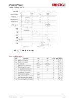
Page 37: ...dware Manual V1 02 01 03 09 2000 2009 BECK IPC GmbH Page 37 8 3 AC Characteristics 8 3 1 Muxed Mode Figure 8 1 Timing Diagram MUXed Mode Rastereinstellungen Abstand horizontal 0 15 Abstand vertikal 0...

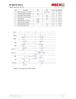
Page 38: ...IPC CHIP SC2x3 Hardware Manual V1 02 01 03 09 2000 2009 BECK IPC GmbH Page 38 Figure 8 2 Timing Diagram MUXed Mode 8 3 2 Non Muxed Mode...

Page 39: ...IPC CHIP SC2x3 Hardware Manual V1 02 01 03 09 2000 2009 BECK IPC GmbH Page 39 Figure 8 3 Timing Diagram Non MUXed Mode...

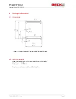
Page 40: ...kage Information 9 1 Dimensions Figure 9 1 Package Dimensions Top view through the conductor board 9 2 SC2x3 Connector Board to Board connection via a 120 pole connector with 0 8 mm spacing Manufactur...

Page 41: ...o program images to the SC2x3 Chiptool can be started and configured through command line parameters This can be used to remote chiptool from other applications to program SC2x3 in series with high qu...

Page 42: ...ions appearing in BECK IPC GmbH Terms and Conditions of Sale only BECK IPC GmbH MAKES NO WARRANTY EXPRESS STATUTORY IMPLIED OR BY DESCRIPTION REGARDING THE INFORMATION SET FORTH HEREIN OR REGARDING TH...

Reviews: