THEORY OF OPERATION
FCS MODULE CIRCUITRY
2 - 4
I-E96-314A
®
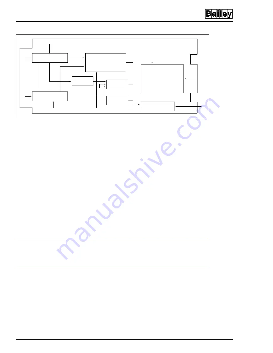
The input enters the board via the P3 connector. The input sig-
nal conditioning circuit chops and squares the AC input into
TTL digital levels, making it electrically compatible with the
MCU. This digital signal is fed to the MCU interrupt. As the
microcontroller detects pulses, it increments the event counter
and memorizes the count in an internal timer. After a 20 ms
period, the MCU writes the count and time interval value to the
double buffered storage area and sets a status bit to tell the
MFP current data is available. The data is double buffered
such that the MCU will not overwrite current data when the
MFP is reading that data. The MFP clocks the data from the
doubled buffered storage area to the slave expander bus inter-
face when it is ready to receive count and timer information.
The sequencing logic prevents the MCU and MFP from access-
ing the storage area simultaneously. The MCU posts the mod-
ule status in the module status buffer. Module status is always
available to the processor module through the slave expander
bus interface.
FCS MODULE CIRCUITRY
The following text explains the operation of the eight functional
blocks that make up the frequency counter slave module.
Input Signal Conditioning
The FCS receives the input signal through its cable connection
to the termination unit. The incoming signal is an analog wave-
form. The input signal conditioning circuit changes the analog
input into a digital input usable by the MCU. Figure
shows
the input signal conditioning circuit and how the circuit con-
verts input signals into a digital waveform.
Figure 2-2. Block Diagram - FCS Module
MCU
SEQUENCING LOGIC
XBUS I/O
XBUS ADD
MOD STAT
WATCHDOG
INPUT SIGNAL
CONDITIONING
TP50148A
DOUBLE BUFFERED
AND LATCHED DATA


