13
Audial USB board
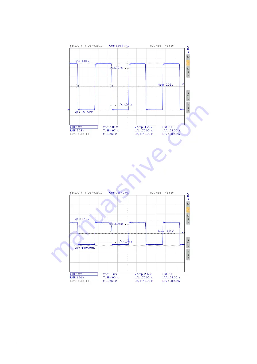
Fig 10: 2.8224 MHz bit clock, BNC output, 12 pF load, no termination
Fig 11: 2.8224 MHz bit clock, BNC output, 75 Ohm ǁ 12 pF load
Page 1: ...USB board Mk2 INSTRUCTION MANUAL Revision 0 December 2017...
Page 2: ...essive heat or mechanical force 4 Use this device exclusively with specified voltages 5 Unplug the device from the wall outlet during a lighting storm Copyright 2017 Audial d o o www audialonline com...
Page 3: ...e U FL PCB connectors These U FL outputs are 3 3 V level with 50 Ohm build out resistors and they can drive several gates but are not meant to drive terminated lines Modules do not include BNC output...
Page 4: ...till necessary with earlier Windows versions Also this driver provides additional functionality as firmware update ASIO interface buffer length control and can be generally preferred soundwise Users c...
Page 5: ...mplement format and it is clocked on the raising edge of BCK Output formats are graphically shown on the figure 4 page 9 OUTPUT CONNECTIONS The table below shows detailed list of the signals available...
Page 6: ...tember 2017 to add 352 8 kHz and 384 kHz compatibility to the boards with TDA1541 A simultaneous data output and 22 5792 24 576 MHz master clocks Please note that the Windows audio is currently limite...
Page 7: ...chieved by four U FL cables Data L Data R BCK LE while I2S requires three U FL cables Data BCK WS By making these connections the whole set up is ready for operation Two boards should be placed one be...
Page 8: ...s 110 mm width x 120 mm depth There are four mounting holes each 4 mm in diameter located 5 mm from the board back left and front edge and 25 mm from the right edge Center of USB connector is 27 mm fr...
Page 9: ...cture shows USB input connector J101 S PDIF output connector J201 U FL output connectors J202 J210 BNC output connectors J301 J307 transformer connections AC1 AC2 LED indicators D10 D101 D102 and moun...
Page 10: ...TA RIGHT TDA1541 A simultaneous data split channels 16 bit data is offset binary MSB MSB LE WCLK BCK DATA LEFT DATA RIGHT PCM1704 split channels 24 bit LSB right justi ed MSB MSB BCK LSB RIGHT CHANNEL...
Page 11: ...Fig 6 24 576 MHz master clock U FL output 12 pF load Fig 7 2 8224 MHz bit clock U FL output 12 pF load 11 Audial USB board...
Page 12: ...Fig 8 2 8224 MHz bit clock U FL output spectral analysis 200 kHz span Fig 9 1 4112 MHz bit clock U FL output spectral analysis 100 kHz span 12 Audial USB board Mk2...
Page 13: ...13 Audial USB board Fig 10 2 8224 MHz bit clock BNC output 12 pF load no termination Fig 11 2 8224 MHz bit clock BNC output 75 Ohm 12 pF load...
Page 14: ...14 Audial USB board Mk2 Fig 12 1 4112 MHz bit clock BNC output spectral analysis 50 kHz span...
Page 15: ......
Page 16: ...Copyright 2017 Audial d o o...