background image

AVR180

3

• Alternative 3: High accuracy. High-quality semiconductor 

ICs are used to build an accurate brown-out detector 
with low-power consumption.

Design Hint: Supply Voltage Filtering

Use low impedance capacitors (low ESR and ESL) on the
V

CC

 and multi-layer PCB with power planes to improve

transient rejection from the power supply.

Alternative 1: Low-Power Consumption

Characteristics

Very Low-Power Consumption, (Typ 0.5

µ

A@3V, 1

µ

A@5V)

Low-Cost

Large Hysteresis, Typ. 0.3 Volts

Fast Output Transitions

Accuracy 

±

 5-10%

High Component Count

Long Response Time on V

CC

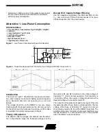
Figure 1.  Low-Power Consumption Brown-Out Detector

Figure 2.  These Oscilloscope Plots Show How the Voltage on RESET Varies with V

CC

Introduction

The circuit in Figure 1 benefits from low-power consump-
tion, which makes it suitable for battery operated applica-
tions. Standard discrete components give a low cost
design.

The voltage transition on the RESET pin is very steep.
Combined with the large hysteresis, the accuracy is high.
On the other hand, the response time is slow, which makes
it unsuitable for rapidly varying supply voltages.

Theory of Operation

This detector has two stages, the detector and the ampli-
fier. In the detector stage, the threshold voltage is set by

the resistors R1 and R2 in relation to the critical voltage of
transistor T1. Under normal operation, this transistor is
conducting, When the supply voltage drops below the
threshold voltage, the transistor shuts off. 

The output from this detector is lead to the input of the ultra
low power amplifier stage. Under normal operation, the low
voltage of the base of transistor T2 causes it to remain
shut, allowing resistor R5 to pull the RESET input high. The
amplifier stage also contains a hysteresis feedback loop
through transistor T3, shorting resistor R3 in the amplifier
when the RESET output is kept low.

V

CC

C3

R1

R2

R3

R4

R5

ISP

AVR

V

CC

100 - 500K 

GND

OPTIONAL
RESET
SWITCH

RESET

T2

C2

T1

C1

T3

<50K 

Summary of Contents for AVR180

Page 1: ...e instructions the supplied volt age must always stay above the mini mum voltage level set by the chosen operating frequency When supplied voltage drops below this level the CPU may start to execute s...

Page 2: ...s described in the introduction may initialize an unintended write to the non volatile memory This may cause random corruption of the memory contents Note 1 As the AVR CPU is not capable of writing to...

Page 3: ...ost design The voltage transition on the RESET pin is very steep Combined with the large hysteresis the accuracy is high On the other hand the response time is slow which makes it unsuitable for rapid...

Page 4: ...ly large current C1 and C2 Capacitors C1 and C2 short RF noise picked up in the cir cuitry and amplified by the transistors Both capacitors can be omitted but a value greater than 1nF is recommended F...

Page 5: ...tor R5 is usually chosen much smaller than the other resistors R1 R4 the last two expressions both sim plify to I VCC R1 R2 R3 R4 VCC 1 R1 R2 1 R3 R4 I VCC R1 R2 R3 R4 R5 R RESET I VCC R1 R2 R5 R RESE...

Page 6: ...transistor T1 is open keeping RESET at VCC When the supply voltage VCC drops below the threshold voltage VT the transistor T1 closes This allows resistor R3 to pull RESET low active The closing of th...

Page 7: ...ide the transistor T1 and pull the RESET pin low To ensure proper low voltage detector operation the series resistance in R3 R4 should not exceed the recommended 50 k Threshold Accuracy As the thresho...

Page 8: ...e reset is held active for a defined amount of time after the condition power on reset brown out reset etc that caused the reset has returned to normal see Figure 6 Some of these devices also provide...

Page 9: ...nput pin is higher than the reference voltage the output will be activated The threshold voltage is easily defined by a volt age divider R1 and R2 Notes 1 Offered by Maxim Integrated Product Inc 2 Off...

Page 10: ...AVR180 10...

Page 11: ...AVR180 11...

Page 12: ...port devices or systems Atmel Headquarters Atmel Operations Corporate Headquarters 2325 Orchard Parkway San Jose CA 95131 TEL 408 441 0311 FAX 408 487 2600 Europe Atmel U K Ltd Coliseum Business Centr...

Reviews: