90
7598H–AVR–07/09
ATtiny25/45/85
14.1.11
Timer/Counter1 in PWM Mode
When the PWM mode is selected, Timer/Counter1 and the Output Compare Register C -
OCR1C form a dual 8-bit, free-running and glitch-free PWM generator with outputs on the
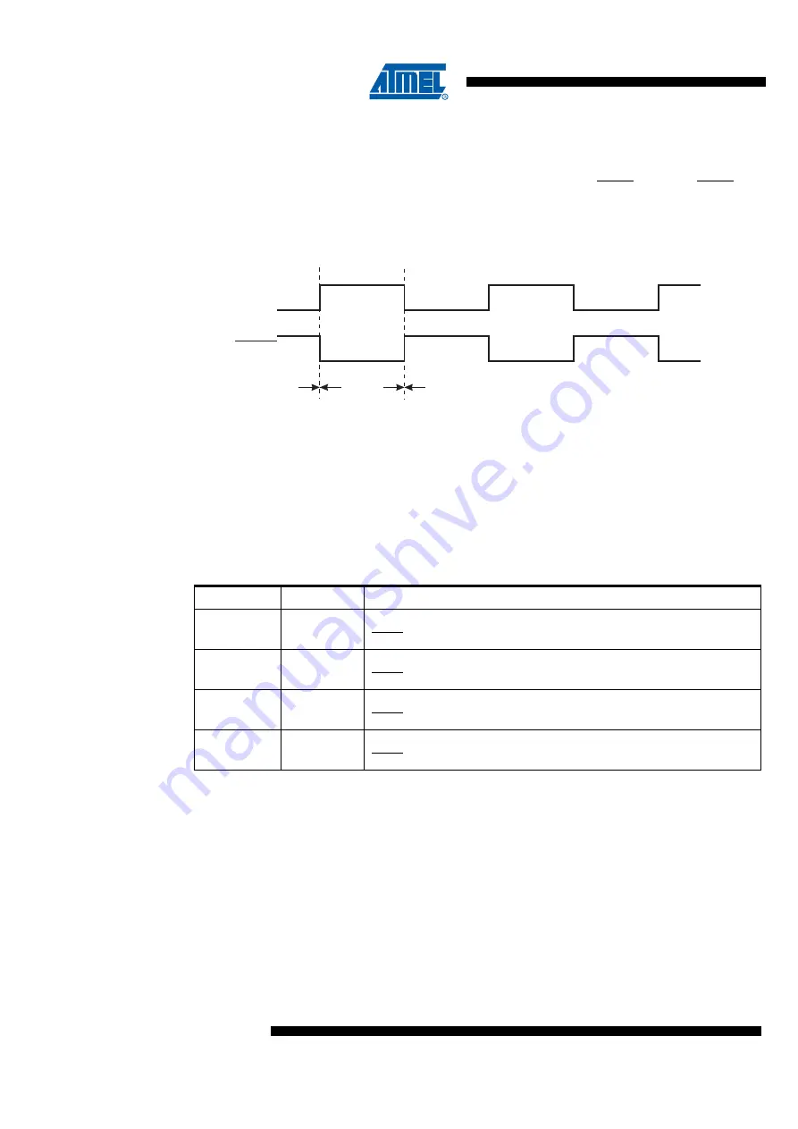
PB1(OC1A) and PB3(OC1B) pins and inverted outputs on pins PB0(OC1A) and PB2(OC1B). As
default non-overlapping times for complementary output pairs are zero, but they can be inserted
using a Dead Time Generator (see description on page 100).
Figure 14-4. The PWM Output Pair
When the counter value match the contents of OCR1A or OCR1B, the OC1A and OC1B outputs
are set or cleared according to the COM1A1/COM1A0 or COM1B1/COM1B0 bits in the
Timer/Counter1 Control Register A - TCCR1, as shown in
.
Timer/Counter1 acts as an up-counter, counting from $00 up to the value specified in the output
compare register OCR1C, and starting from $00 up again. A compare match with OC1C will set
an overflow interrupt flag (TOV1) after a synchronization delay following the compare event.
Note that in PWM mode, writing to the Output Compare Registers OCR1A or OCR1B, the data
value is first transferred to a temporary location. The value is latched into OCR1A or OCR1B
when the Timer/Counter reaches OCR1C. This prevents the occurrence of odd-length PWM
pulses (glitches) in the event of an unsynchronized OCR1A or OCR1B. See
example.
Table 14-4.
Compare Mode Select in PWM Mode
COM11
COM10
Effect on Output Compare Pins
0
0
OC1x not connected.
OC1x not connected.
0
1
OC1x cleared on compare match. Set whenTCNT1 = $01.
OC1x set on compare match. Cleared when TCNT1 = $00.
1
0
OC1x cleared on compare match. Set when TCNT1 = $01.
OC1x not connected.
1
1
OC1x Set on compare match. Cleared when TCNT1= $01.
OC1x not connected.
PWM1x
PWM1x
x = A or B
t
non-overlap
=0
t
non-overlap
=0


