background image

OSC

EXF2

TF2

T2EX  PIN

COUNT
DIRECTION
1=UP
0=DOWN

T2  PIN

TR2

CONTROL

OVERFLOW

(DOWN  COUNTING  RELOAD  VALUE)

(UP  COUNTING  RELOAD  VALUE)

TOGGLE

TIMER  2

INTERRUPT

12

RCAP2L

RCAP2H

0FFH

0FFH

TH2

TL2

C/T2  =  0

C/T2  =  1

÷

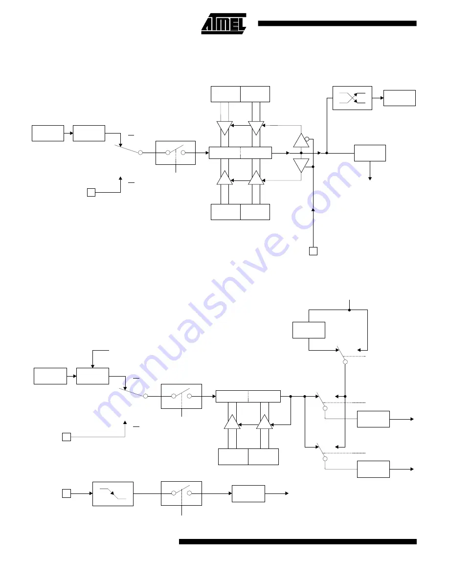
Figure 3.  Timer 2 Auto Reload Mode (DCEN = 1)

OSC

SMOD1

RCLK

TCLK

Rx

CLOCK

Tx

CLOCK

T2EX  PIN

T2  PIN

TR2

CONTROL

"1"

"1"

"1"

"0"

"0"

"0"

TIMER  1  OVERFLOW

NOTE: OSC. FREQ. IS  DIVIDED  BY  2,  NOT  12

TIMER  2

INTERRUPT

2

2

6

16

RCAP2L

RCAP2H

TH2

TL2

C/T2  =  0

C/T2  =  1

EXF2

CONTROL

TRANSITION

DETECTOR

EXEN2

÷

÷

÷

÷

Figure 4.  Timer 2 in Baud Rate Generator Mode

8

AT89C52

Summary of Contents for AT89C52

Page 1: ...ry to be reprogrammed in system or by a conventional nonvolatile memory programmer By combining a versatile 8 bit CPU with Flash on a monolithic chip the Atmel AT89C52 is a powerful microcomputer which provides a highly flexible and cost effective solution to many embedded control applications continued 2 3 1 I N D E X C O R N E R 3 4 P 1 0 T 2 V C C P 1 1 T 2 E X P 1 2 P 1 3 N C 4 2 4 3 4 0 4 1 6...

Page 2: ...COUNTER DPTR RAM ADDR REGISTER INSTRUCTION REGISTER B REGISTER INTERRUPT SERIAL PORT AND TIMER BLOCKS STACK POINTER ACC TMP2 TMP1 ALU PSW TIMING AND CONTROL PORT 3 LATCH PORT 3 DRIVERS P3 0 P3 7 PORT 1 LATCH PORT 1 DRIVERS P1 0 P1 7 OSC GND VCC PSEN ALE PROG EA VPP RST PORT 0 DRIVERS P0 0 P0 7 Block Diagram 2 AT89C52 ...

Page 3: ...are reset Description Continued Port 1 also receives the low order address bytes during Flash programming and program verification Port 2 Port 2 is an 8 bit bidirectional I O port with internal pullups The Port 2 output buffers can sink source four TTL inputs When 1s are written to Port 2 pins they are pulled high by the internal pullups and can be used as inputs As inputs Port 2 pins that are ext...

Page 4: ...e the device to fetch code from external pro gram memory locations starting at 0000H up to FFFFH Note however that if lock bit 1 is programmed EA will be internally latched on reset EA should be strapped to VCC for internal program execu tions This pin also receives the 12 volt programming enable voltage VPP during Flash programming when 12 volt pro gramming is selected XTAL1 Input to the invertin...

Page 5: ...re mode or 16 bit auto reload mode Interrupt Registers The individual interrupt enable bits are in the IE register Two priorities can be set for each of the six interrupt sources in the IP register Table 2 T2CON Timer Counter 2 Control Register T2CON Address 0C8H Reset Value 0000 0000B Bit Addressable TF2 EXF2 RCLK TCLK EXEN2 TR2 C T2 CP RL2 Bit 7 6 5 4 3 2 1 0 Symbol Function TF2 Timer 2 overflow...

Page 6: ...t T2EX causes bit EXF2 in T2CON to be set The EXF2 bit like TF2 can generate an interrupt The capture mode is illustrated in Figure 1 Auto Reload Up or Down Counter Timer 2 can be programmed to count up or down when configured in its 16 bit auto reload mode This feature is invoked by the DCEN Down Counter Enable bit located in the SFR T2MOD see Table 4 Upon reset the DCEN bit is set to 0 so that t...

Page 7: ...ansition at external input T2EX This transition also sets the EXF2 bit Both the TF2 and EXF2 bits can generate an interrupt if enabled Setting the DCEN bit enables Timer 2 to count up or down as shown in Figure 3 In this mode the T2EX pin controls the direction of the count A logic 1 at T2EX makes Timer 2 count up The timer will overflow at 0FFFFH and set the TF2 bit This overflow also causes the ...

Page 8: ...CAP2H 0FFH 0FFH TH2 TL2 C T2 0 C T2 1 Figure 3 Timer 2 Auto Reload Mode DCEN 1 OSC SMOD1 RCLK TCLK Rx CLOCK Tx CLOCK T2EX PIN T2 PIN TR2 CONTROL 1 1 1 0 0 0 TIMER 1 OVERFLOW NOTE OSC FREQ IS DIVIDED BY 2 NOT 12 TIMER 2 INTERRUPT 2 2 6 16 RCAP2L RCAP2H TH2 TL2 C T2 0 C T2 1 EXF2 CONTROL TRANSITION DETECTOR EXEN2 Figure 4 Timer 2 in Baud Rate Generator Mode 8 AT89C52 ...

Page 9: ...e at 1 2 the oscilla tor frequency The baud rate formula is given below Modes1 and 3 Baud Rate Oscillator Frequency 32 x 65536 RCAP2H RCAP2L where RCAP2H RCAP2L is the content of RCAP2H and RCAP2L taken as a 16 bit unsigned integer Timer 2 as a baud rate generator is shown in Figure 4 This figure is valid only if RCLK or TCLK 1 in T2CON Note that a rollover in TH2 does not set TF2 and will not gen...

Page 10: ...ecial Function Register IE IE also contains a global disable bit EA which disables all interrupts at once Note that Table 5 shows that bit position IE 6 is unimple mented In the AT89C51 bit position IE 5 is also unimple mented User software should not write 1s to these bit po sitions since they may be used in future AT89 products Timer 2 interrupt is generated by the logical OR of bits TF2 and EXF...

Page 11: ...dware inhib its access to internal RAM in this event but access to the port pins is not inhibited To eliminate the possibility of an unexpected write to a port pin when idle mode is termi nated by a reset the instruction following the one that in vokes idle mode should not write to a port pin or to external memory Power Down Mode In the power down mode the oscillator is stopped and the instruction...

Page 12: ...e table and Figures 9 and 10 To program the AT89C52 take the following steps 1 Input the desired memory location on the address lines 2 Input the appropriate data byte on the data lines 3 Activate the correct combination of control signals 4 Raise EA VPP to 12 V for the high voltage program ming mode 5 Pulse ALE PROG once to program a byte in the Flash array or the lock bits The byte write cycle i...

Page 13: ...must be executed before the code memory can be reprogrammed Reading the Signature Bytes The signature bytes are read by the same procedure as a normal verification of locations 030H 031H and 032H except that P3 6 and P3 7 must be pulled to a logic low The values returned are as follows 030H 1EH indicates manufactured by Atmel 031H 52H indicates 89C52 032H FFH indicates 12 V programming 032H 05H in...

Page 14: ...dth 1 110 µs tAVQV Address to Data Valid 48tCLCL tELQV ENABLE Low to Data Valid 48tCLCL tEHQV Data Float After ENABLE 0 48tCLCL tGHBL PROG High to BUSY Low 1 0 µs tWC Byte Write Cycle Time 2 0 ms Note 1 Only used in 12 volt programming mode P1 P2 6 P3 6 P2 0 P2 4 A0 A7 ADDR OOOOH 1FFFH SEE FLASH PROGRAMMING MODES TABLE 4 24 MHz A8 A12 P0 5V P2 7 PGM DATA PROG V V IH PP VIH ALE P3 7 XTAL 2 EA RST P...

Page 15: ...ON ADDRESS DATA IN DATA OUT Flash Programming and Verification Waveforms Low Voltage Mode tGLGH tGHSL tAVGL tSHGL tDVGL tGHAX tAVQV tGHDX tEHSH tELQV tWC BUSY READY tGHBL tEHQZ P1 0 P1 7 P2 0 P2 4 P3 0 ALE PROG PORT 0 LOGIC 1 LOGIC 0 EA VPP VPP P2 7 ENABLE P3 4 RDY BSY PROGRAMMING ADDRESS VERIFICATION ADDRESS DATA IN DATA OUT Flash Programming and Verification Waveforms High Voltage Mode AT89C52 1...

Page 16: ...z TA 25 C 10 pF ICC Power Supply Current Active Mode 12 MHz 25 mA Idle Mode 12 MHz 6 5 mA Power Down Mode 2 VCC 6 V 100 µA VCC 3 V 40 µA Operating Temperature 55 C to 125 C Storage Temperature 65 C to 150 C Voltage on Any Pin with Respect to Ground 1 0 V to 7 0 V Maximum Operating Voltage 6 6 V DC Output Current 15 0 mA NOTICE Stresses beyond those listed under Absolute Maxi mum Ratings may cause ...

Page 17: ...truction In 312 5tCLCL 55 ns tPLAZ PSEN Low to Address Float 10 10 ns tRLRH RD Pulse Width 400 6tCLCL 100 ns tWLWH WR Pulse Width 400 6tCLCL 100 ns tRLDV RD Low to Valid Data In 252 5tCLCL 90 ns tRHDX Data Hold After RD 0 0 ns tRHDZ Data Float After RD 97 2tCLCL 28 ns tLLDV ALE Low to Valid Data In 517 8tCLCL 150 ns tAVDV Address to Valid Data In 585 9tCLCL 165 ns tLLWL ALE Low to RD or WR Low 200...

Page 18: ...SEN RD PORT 0 PORT 2 P2 0 P2 7 OR A8 A15 FROM DPH A0 A7 FROM PCL A8 A15 FROM PCH DATA IN INSTR IN External Data Memory Read Cycle tLHLL tLLIV tPLIV tLLAX tPXIZ tPLPH tPLAZ tPXAV tAVLL tLLPL tAVIV tPXIX ALE PSEN PORT 0 PORT 2 A8 A15 A0 A7 A0 A7 A8 A15 INSTR IN External Program Memory Read Cycle 18 AT89C52 ...

Page 19: ... Rise Time 20 ns tCHCL Fall Time 20 ns tCHCX tCHCX tCLCX tCLCL tCHCL tCLCH V 0 5V CC 0 45V 0 2 V 0 1V CC 0 7 VCC External Clock Drive Waveforms tLHLL tLLWL tLLAX tWHLH tAVLL tWLWH tAVWL tQVWX tQVWH tWHQX A0 A7 FROM RI OR DPL ALE PSEN WR PORT 0 PORT 2 P2 0 P2 7 OR A8 A15 FROM DPH A0 A7 FROM PCL A8 A15 FROM PCH DATA OUT INSTR IN External Data Memory Cycle AT89C52 19 ...

Page 20: ...Conditions The values in this table are valid for VCC 5 0 V 20 and Load Capacitance 80 pF Symbol Parameter 12 MHz Osc Variable Oscillator Units Min Max Min Max tXLXL Serial Port Clock Cycle Time 1 0 12tCLCL µs tQVXH Output Data Setup to Clock Rising Edge 700 10tCLCL 133 ns tXHQX Output Data Hold After Clock Rising Edge 50 2tCLCL 33 ns tXHDX Input Data Hold After Clock Rising Edge 0 0 ns tXHDV Cloc...

Page 21: ... 12LM 44L 55 C to 125 C AT89C52 12DM 883 40D6 Military 883C AT89C52 12LM 883 44L Class B Fully Compliant 55 C to 125 C 16 5 V 20 AT89C52 16AC 44A Commercial AT89C52 16JC 44J 0 C to 70 C AT89C52 16PC 40P6 AT89C52 16QC 44Q AT89C52 16AI 44A Industrial AT89C52 16JI 44J 40 C to 85 C AT89C52 16PI 40P6 AT89C52 16QI 44Q AT89C52 16AA 44A Automotive AT89C52 16JA 44J 40 C to 125 C AT89C52 16PA 40P6 AT89C52 1...

Page 22: ...Leadless Chip Carrier LCC 40P6 40 Lead 0 600 Wide Plastic Dual Inline Package PDIP 44Q 44 Lead Plastic Gull Wing Quad Flatpack PQFP Ordering Information Speed MHz Power Supply Ordering Code Package Operation Range 24 5 V 20 AT89C52 24AC 44A Commercial AT89C52 24JC 44J 0 C to 70 C AT89C52 24PC 44P6 AT89C52 24QC 44Q AT89C52 24AI 44A Industrial AT89C52 24JI 44J 40 C to 85 C AT89C52 24PI 44P6 AT89C52 ...

Reviews: