


GENERAL INFORMATION
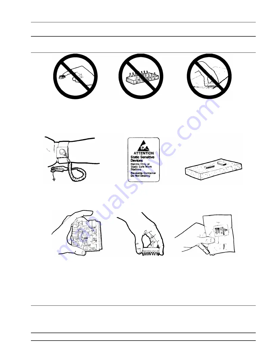
STATIC SENSITIVE COMPONENT HANDLING
PROCEDURES
37XXXD MM
1-11
1.
Do not touch exposed contacts on
any static sensitive component.
2.
Do not slide static sensitive com-
ponent across any surface.
3.
Do not handle static sensitive com-
ponents in areas where the floor or
work surface covering is capable of
generating a static charge.
4.
Wear a static-discharge wristband
when working with static sensitive
components.
5.
Label all static sensitive devices.
6.
Keep component leads shorted to-
gether whenever possible.
7.
Handle PCBs only by their edges.
Do not handle by the edge connec-
tors.
8.
Lift & handle solid state devices by
their bodies – never by their leads.
9.
Transport and store PCBs and
other static sensitive devices in
static-shielded containers.
10.
ADDITIONAL PRECAUTIONS:
·
Keep workspaces clean and free of any objects capable of holding or storing a static charge.
·
Connect soldering tools to an earth ground.
·
Use only special anti-static suction or wick-type desoldering tools.
Figure 1-2.
Static Sensitive Component Handling Procedures
Summary of Contents for 37 D Series
Page 3: ......
Page 4: ......
Page 12: ......
Page 14: ...1 2 37XXXD MM Figure 1 1 Series 37XXXD Vector Network Analyzer System...
Page 26: ......
Page 36: ......
Page 38: ......
Page 62: ......
Page 80: ......
Page 82: ......
Page 90: ......
Page 104: ......
Page 122: ......
Page 148: ......
Page 152: ......
Page 154: ......
Page 156: ......
Page 158: ......
Page 184: ......
Page 190: ......


