A8520E24A91 – User’s Manual
Page 31 of 34
Release Date 02/27/12
BL_FLASH_MASS_ERASE();
Check SWR Proceed only if SWR matches required value (Reset device and Restart
programming again)
// For each flash page
for (int n = 0; n < 31; n++) {
// Write page data to the start of the available RAM area
SET_ADDR(0x6000, sw);
WRITE(0x400, data to be programmed into flash page n , sw);
/* While using the image generated by TI- Purepath Wireless Configurator, note that the entire
image file generated by PWC-TI is Intel_hex format. For programming 8520 module use only
the data and discard additional data/information */
// Program the page
BL_FLASH_PROG_PAGE(RAM_ADDR = 0x6000, FLASH_ADDR = (n*0x400))
Check SWR Proceed only if SWR matches required value wait till the block is completely
transfered
}
// Verify the flash contents
BL_FLASH_VERIFY(BYTE_COUNT = value read from the HEX file );
/* The flash verify byte count data is 4 byte value stored from location &h 8010 within the image
file */
Check SWR Proceed only if SWR matches required value (Reset device and Restart
programming again)
SYS_RESET()
// Done, perform SYS_RESET() to start the application
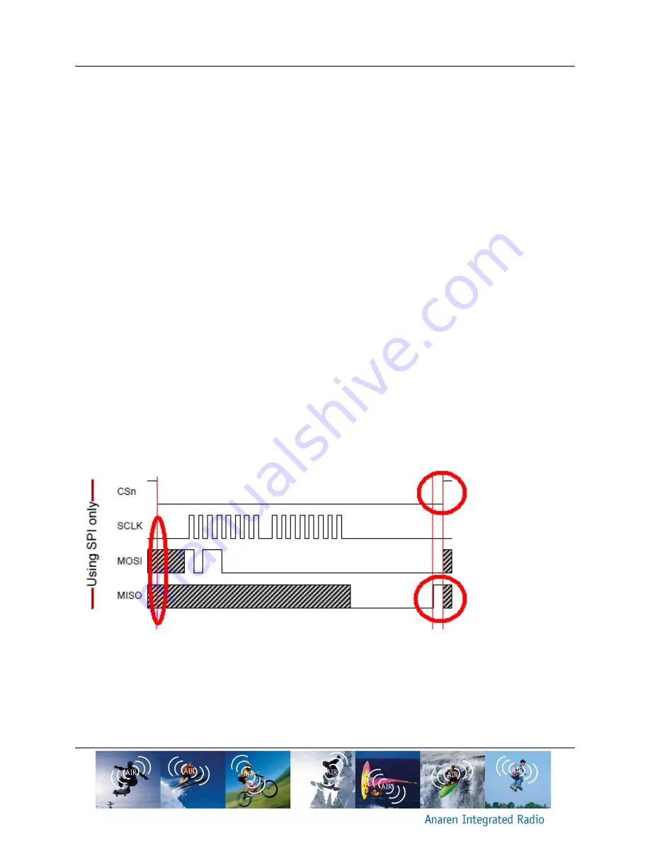
If the status word read fails immediately after execution of BOOT_RESET or BL_UNLOCK_SPI
then it is most likely due to the special SPI requirement during these instructions as MISO must
go low and then high after the SPI clock sequence as shown in the figure below.
Figure 12 SPI clock sequence
If the SPI bus controller is unable to perform this wait, then use the SPI pins as GPIO’s and
manually program the bit sequences as described below for the BOOT_RESET().
Procedure for programming Boot_Reset()
1. Assert CSn Low and then clock the SCL with each negative edge of clock asset the logic
level to high or low on MOSI pin.


