background image

User Guide

UG-1533

ACE SOFTWARE OPERATION

analog.com

Rev. A | 11 of 30

LAUNCHING THE SOFTWARE

After the EVAL-ADAQ4001FMCZ or EVAL-ADAQ4003FMCZ and

the 

SDP-H1

 are properly connected to the PC, launch the 

ACE

evaluation software by taking the following steps:

1.

From the 

Start

 menu of the PC, click 

All Programs > Analog

Devices > ACE> ACE.exe

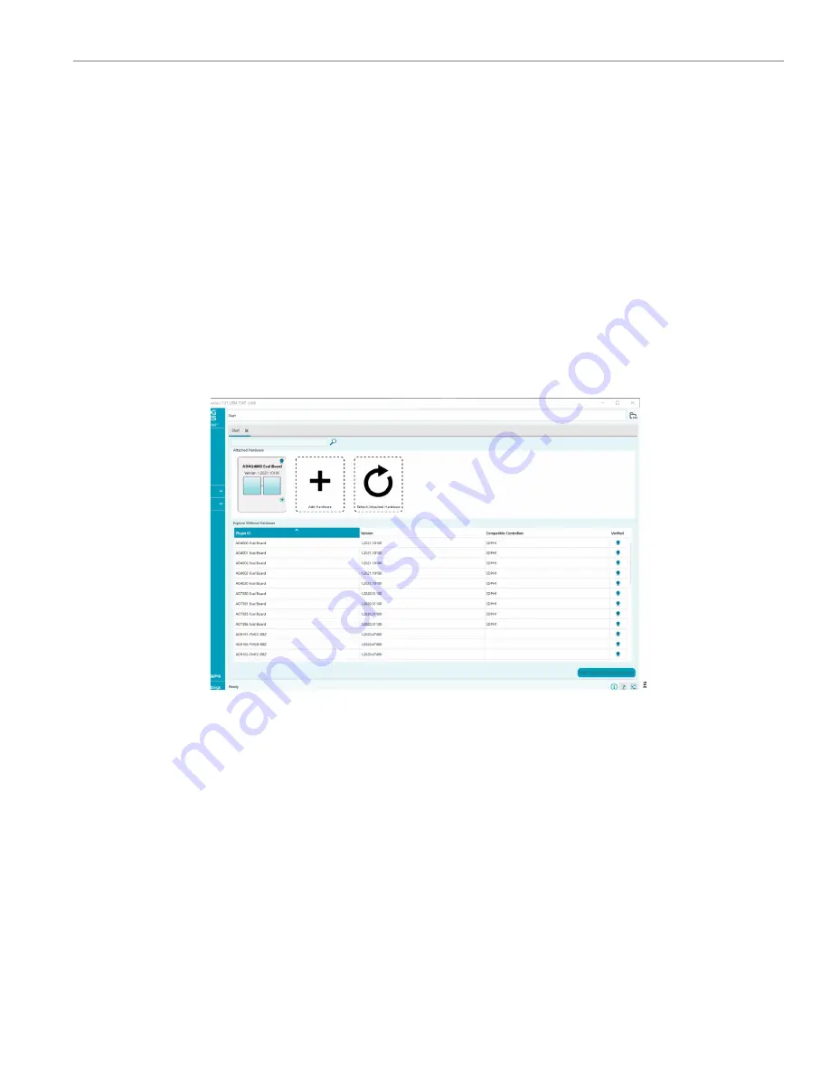
 to open the ACE software main

window shown in 

Figure 16

.

2.

Connect the EVAL-ADAQ4001FMCZ or EVAL-

ADAQ4003FMCZ and the SDP-H1 to the USB. If the EVAL-

ADAQ4001FMCZ or EVAL-ADAQ4003FMCZ is not connected

to the USB port via the SDP-H1 when the software launch-

es, the 

ADAQ4001 Eval Board

 or 

ADAQ4003 Eval Board

icon does not appear in the 

Attached Hardware

 section.

To make the 

ADAQ4001 Eval Board

 or 

ADAQ4003 Eval

Board

 icon appear, connect the EVAL-ADAQ4001FMCZ or

EVAL-ADAQ4003FMCZ and the SDP-H1 to the USB port of the

PC, wait a few seconds, and then follow the instructions in the

dialog box that opens.

3.

Double click the 

ADAQ4001 Eval Board

 or 

ADAQ4003 Eval

Board

 icon in the ACE software main window (see 

Figure 16

)

to open the board view window shown in 

Figure 17

.

4.

Double click the 

ADAQ4001

 or 

ADAQ4003

 chip icon in the

board view window (see 

Figure 17

) to open the chip view

window shown in 

Figure 18

. The on-board voltage reference

provided by the 

ADR4550

 is 5.0 V, as shown in the board

view window. Type the value of the reference voltage in the

reference voltage box in the chip view window when using the

external reference.

5.

Click

 Software Defaults

 and then click 

Apply Changes

 to

apply the default settings.

6.

Click the 

Proceed to Analysis

 button to show the 

Analysis

view window, as shown in 

Figure 19

.

Figure 16. ACE Software Main Window

Summary of Contents for EVAL-ADAQ4001FMCZ

Page 1: ...DZ or EVAL ADAQ4003PMDZ peripheral module Pmod board and the EVAL PMD IB1Z Pmod to field programmable grid array FPGA mezzanine card FMC interposer board that interfaces with the system demonstration controller board EVAL SDP CH1Z via a 160 pin FMC connector as shown in Figure 1 The ADAQ4001 µModule and ADAQ4003 µModule combine multi ple common signal processing and conditioning blocks into a sing...

Page 2: ...rdering Information 28 Bill of Materials 28 REVISION HISTORY 5 2021 Rev 0 to Rev A Added EVAL ADAQ4001FMCZ 1 Added ADAQ4001 1 Added EVAL ADAQ4001PMDZ 1 Changes to Software Needed Section 1 Changes to Figure 2 4 Changes to Power Supplies Section 5 Changes to Table 2 6 Changes to Evaluation Board Software Section 8 Added Figure 8 to Figure 14 Renumbered Sequentially 8 Deleted Figure 8 to Figure 20 R...

Page 3: ...User Guide UG 1533 EVAL ADAQ4001FMCZ OR EVAL ADAQ4003FMCZ EVALUATION BOARD KIT PHOTOGRAPH analog com Rev A 3 of 30 Figure 1 ...

Page 4: ... EVAL SDP CH1Z SDP H1 BOARD The EVAL ADAQ4001FMCZ and EVAL ADAQ4003FMCZ evalua tion kit uses a serial port interface SPI and requires the system demonstration platform SDP H1 to capture the data via a graphic user interface GUI see Figure 1 The SDP H1 requires power from a 12 V wall adapter The SDP H1 has a Xilinx Spartan 6 and an ADSP BF527 processor with connectivity to the PC through a USB 2 0 ...

Page 5: ...f the high frequency noise interference In addition the EVAL ADAQ4001PMDZ and EVAL ADAQ4003PMDZ can be powered from a benchtop power supply of 15 5 V The 15 5 V 15 5 V and GND test points are available on board to support this function When bench power is used the on board power supplies are no longer required and the link between the output pin of the ADP5070 must be removed that is uninstall R20...

Page 6: ... for other gains JP3 B1 and B2 A1 and A2 µModule input The ADAQ4001 or ADAQ4003 has a gain of 0 454 22 V range See the ADAQ4001 or the ADAQ4003 data sheet for other gains JP4 Pin A to Pin COM Synchronize the switching frequency to CNV To set the switching frequency to 1 2 MHz pull the SYNC FREQ pin of the ADP5070 low or Pin B to Pin COM JP5 Pin A to Pin COM Op amp or in amp Connect the J1 input to...

Page 7: ... Figure 6 Gain 1 Figure 7 Gain 1 9 Table 3 The Different Gain Positions Available for the Links of the EVAL ADAQ4001PMDZ or EVAL ADAQ4003PMDZ Gain Input Range V Input Signal on Pins Test Conditions 0 454 11 R1K1 and R1K1 For JP2 tie A1 to A2 and tie B1 to B2 and for JP3 tie A1 to A2 and tie B1 to B2 see Figure 4 0 9 5 5 R1K1 and R1K1 For JP2 tie B1 to B2 and for JP3 tie B1 to B2 see Figure 5 1 5 R...

Page 8: ...H1 to the USB port of the PC to ensure that the evaluation system is properly recognized when it is connected to the PC Installing the ACE Evaluation Software To install the ACE evaluation software take the following steps 1 Download the ACE software to a Windows based PC 2 Double click the ACEInstall exe file to begin the installation By default the ACE software is saved to the following location...

Page 9: ...stalling the ACE software take the following steps to set up the EVAL ADAQ4001FMCZ or EVAL ADAQ4003FMCZ and the SDP H1 1 Ensure that all configuration links are in the appropriate posi tions as detailed from Figure 4 to Figure 7 2 Connect the EVAL ADAQ4001FMCZ or EVAL ADAQ4003FMCZ securely to the 160 way connector on the SDP H1 The EVAL ADAQ4001FMCZ and EVAL ADAQ4003FMCZ do not require an external...

Page 10: ...operly connected to the PC Analog Devices SDP H1 is shown in the ADI Devel opment Tools list in the Device Manager window as shown in Figure 15 Figure 15 Device Manager Window Disconnecting the EVAL ADAQ4001FMCZ or EVAL ADAQ4003FMCZ Disconnect power from the SDP H1 or press the reset tact switch located alongside the mini USB port on the SDP H1 before dis connecting the EVAL ADAQ4001FMCZ or EVAL A...

Page 11: ... Eval Board icon appear connect the EVAL ADAQ4001FMCZ or EVAL ADAQ4003FMCZ and the SDP H1 to the USB port of the PC wait a few seconds and then follow the instructions in the dialog box that opens 3 Double click the ADAQ4001 Eval Board or ADAQ4003 Eval Board icon in the ACE software main window see Figure 16 to open the board view window shown in Figure 17 4 Double click the ADAQ4001 or ADAQ4003 c...

Page 12: ...User Guide UG 1533 ACE SOFTWARE OPERATION analog com Rev A 12 of 30 Figure 17 Board View Window Figure 18 Chip View Window ...

Page 13: ...User Guide UG 1533 ACE SOFTWARE OPERATION analog com Rev A 13 of 30 Figure 19 Analysis View Window ...

Page 14: ...e the per formance of the ADAQ4001 or the ADAQ4003 Before performing any measurements set the capture settings see the CAPTURE section and analysis settings see the ANALYSIS SETTINGS sec tion The Analysis view window contains the Waveform tab see Figure 20 Histogram Tab see Figure 21 and FFT tab see Figure 22 Figure 20 Waveform Tab Figure 21 Histogram Tab ...

Page 15: ...the Oversampling Ratio pulldown menu in the Software Oversampling section can be set between 2 and 256 and provide improved signal to noise ratio SNR performance Refer to the ADAQ4001 data sheet and ADAQ4003 data sheet to determine the maximum oversampling ratio for the selected oversampling mode Click Run Once to start a data capture of the samples at the sample rate specified in the No of sample...

Page 16: ...h and the RE SULTS pane as shown in Figure 21 The RESULTS pane displays the information related to the dc performance The Histogram graph displays the number of hits per code within the sampled data This graph is useful for dc analysis and indicates the noise performance of the device FFT TAB The FFT tab displays fast Fourier transform FFT information for the last batch of samples gathered see Fig...

Page 17: ...User Guide UG 1533 ACE SOFTWARE OPERATION analog com Rev A 17 of 30 Figure 24 DNL Tab ...

Page 18: ... port where the SDP H1 cannot read quickly a timeout error may result In this case do not read continuously or lower the number of samples taken HARDWARE TROUBLESHOOTING To troubleshoot the hardware take the following steps 1 Check that the power is applied within the power ranges described in the Setting Up the EVAL ADAQ4001FMCZ and EVAL ADAQ4003FMCZ Evaluation Kit section 2 Using a voltmeter mea...

Page 19: ...ide UG 1533 EVALUATION BOARD SCHEMATICS AND SILKSCREENS analog com Rev A 19 of 30 EVAL ADAQ4001PMDZ AND EVAL ADAQ4003PMDZ Figure 25 EVAL ADAQ4001PMDZ and EVAL ADAQ4003PMDZ Power Supplies and Voltage Reference ...

Page 20: ...VALUATION BOARD SCHEMATICS AND SILKSCREENS analog com Rev A 20 of 30 Figure 26 EVAL ADAQ4001PMDZ and EVAL ADAQ4003PMDZ µModule and Signal Conditioning Figure 27 EVAL ADAQ4001PMDZ and EVAL ADAQ4003PMDZ Silkscreen Top Layer ...

Page 21: ...ARD SCHEMATICS AND SILKSCREENS analog com Rev A 21 of 30 Figure 28 EVAL ADAQ4001PMDZ and EVAL ADAQ4003PMDZ Layer 1 Figure 29 EVAL ADAQ4001PMDZ and EVAL ADAQ4003PMDZ Layer 2 Figure 30 EVAL ADAQ4001PMDZ and EVAL ADAQ4003PMDZ Layer 3 GND ...

Page 22: ...User Guide UG 1533 EVALUATION BOARD SCHEMATICS AND SILKSCREENS analog com Rev A 22 of 30 Figure 31 EVAL ADAQ4001PMDZ and EVAL ADAQ4003PMDZ Layer 4 Secondary ...

Page 23: ...User Guide UG 1533 EVALUATION BOARD SCHEMATICS AND SILKSCREENS analog com Rev A 23 of 30 EVAL PMD IB1Z Figure 32 EVAL PMD IB1Z Interposer Schematic Diagram ...

Page 24: ...User Guide UG 1533 EVALUATION BOARD SCHEMATICS AND SILKSCREENS analog com Rev A 24 of 30 Figure 33 EVAL PMD IB1Z Top Layer ...

Page 25: ...User Guide UG 1533 EVALUATION BOARD SCHEMATICS AND SILKSCREENS analog com Rev A 25 of 30 Figure 34 EVAL PMD IB1Z Silkscreen Primary ...

Page 26: ...User Guide UG 1533 EVALUATION BOARD SCHEMATICS AND SILKSCREENS analog com Rev A 26 of 30 Figure 35 EVAL PMD IB1Z Silkscreen Secondary ...

Page 27: ...User Guide UG 1533 EVALUATION BOARD SCHEMATICS AND SILKSCREENS analog com Rev A 27 of 30 Figure 36 EVAL PMD IB1Z Secondary ...

Page 28: ...µF capacitor 10 10 V X7R 0805 TDK Corporation C2012X7R1A106K125AC 6 C39 to C44 0 1 µF ceramic capacitors X7R general purpose AVX 04023C104KAT2A 2 C4 C9 4 7 µF ceramic capacitors X7R Murata GCM21BR71E105KA56L 1 C52 0 0033 µF monolithic ceramic capacitor 0402 Yageo CC0402KRX7R9BB332 1 C53 0 0047 µF ceramic capacitor X7R general purpose KEMET C0402C472K5RACTU 2 D1 D2 Schottky diodes barrier rectifier...

Page 29: ...ic ERJ 2RKF9532X 1 R9 3 3 kΩ resistor precision thick film chip Panasonic ERJ 2RKF3301X 1 RN1 Resistor network quad matched Analog Devices Inc LT5400BHMS8E 4 PBF 1 U1 Ultralow noise high accuracy 5 0 V voltage reference Analog Devices ADR4550BRZ 1 U2 Dual positive and negative low noise low dropout LDO regulator Analog Devices LT3032IDE PBF 1 U3 1 A 0 6 A dc to dc switching regulator with independ...

Page 30: ...material content of the Evaluation Board Modifications to the Evaluation Board must comply with applicable law including but not limited to the RoHS Directive TERMINATION ADI may terminate this Agreement at any time upon giving written notice to Customer Customer agrees to return to ADI the Evaluation Board at that time LIMITATION OF LIABILITY THE EVALUATION BOARD PROVIDED HEREUNDER IS PROVIDED AS...

Reviews: