


UG-1262
Rev. B | Page 110 of 312
OPEN THIS SWITCH
TO DISCONNECT
POTENTIOSTAT AMP
VZERO0
C = 0.1µF
CE0
RE0
CAP_POT0
VBIAS0
C = ~0.1µF
R
C
C
C
CE0
SE0
R
W
R
E
R
E
C
W
RE0
DE
SW12
SW2
SW3
SW8
–
+
AMP
10kΩ
10kΩ
V
ZERO
DUAL
OUTPUTS
12-BIT VDAC
V
ZERO
V
BIAS
2.4V
VREF_2.5V
0.2V
P5
SW13
D5
–
+
–
+
–
+
–
+
–
+
–
+
–
+
P
N
2R
2R
SW16
SW17
D
A
B
DACN
DACP
DACN
R
R
PGA
RPF
f
C
= 80kHz
12-BIT
DAC
DIG
WAVE
GEN
DAC TO DAC
BUFFERS
1667
5-
023
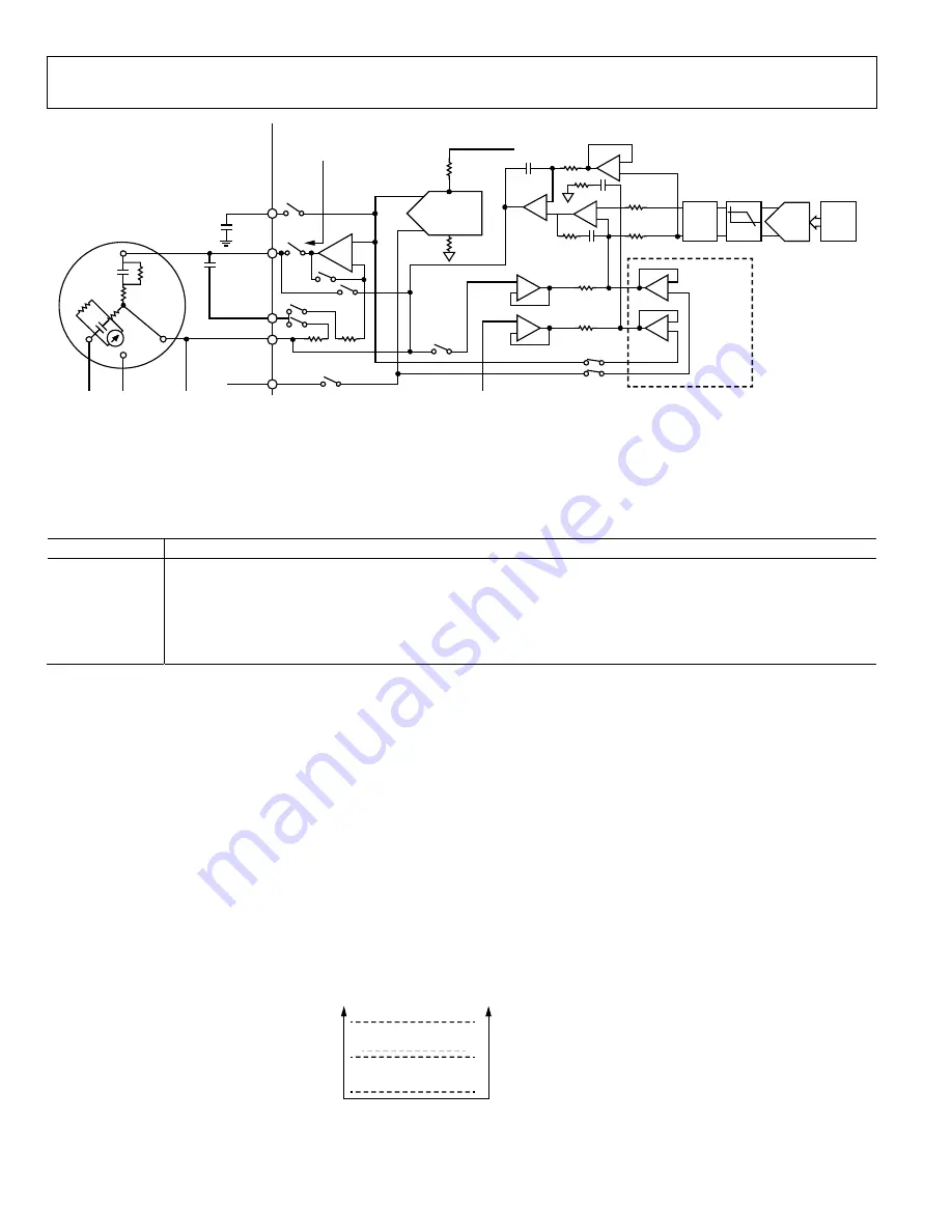
Figure 24. Signal Path for AC Signal Coupled onto DC Level Set by Low Power DAC
AVOIDING INCOHERENCY ERRORS BETWEEN EXCITATION AND MEASUREMENT FREQUENCIES DURING
IMPEDANCE MEASUREMENTS
Table 126 details the recommended settings to avoid incoherency errors between excitation frequencies and measurement frequencies
during impedance measurements.
Table 126. Recommended Settings to Avoid Incoherency Errors
Parameter Recommended
Settings
Hanning
Window
Always on (DFTCON, Bit 0 = 1). Enabling the Hanning window avoids issues due to incoherency. Disabling the Hanning
window can result in degraded performance.
High Speed DAC
Update Rate
In low power mode, the typical value is 16 MHz or 27 MHz. (HSDACCON, Bits[8:1] = 0x1B). In high power mode, the
typical value is 32 MHz or 7 MHz. (HSDACCON, Bits[8:1] = 0x7).
ADC Sampling
Rate
Low power mode, 800 kSPS, high frequency oscillator = 16 MHz. High power mode, 1.6 MSPS, high frequency
oscillator = 32 MHz.
CALIBRATING THE HIGH SPEED DAC
The high speed DAC is not calibrated during production testing. This section describes the calibration of the high speed DAC for all gain
settings in low and high power modes. Calibrate the high speed DAC if it is intended to generate an excitation signal to a sensor. If an
offset error exists on the excitation signal, and a current or voltage output must be measured, the DAC output voltage can exceed the
headroom of the selected TIA or ADC input buffer and PGA setting.
Calibrate the high speed DAC with the required HSDACCON, Bit 12 and HSDACCON, Bit 0 settings. For example, if the DAC is calibrated
with HSDACCON, Bit 12 = 0 and HSDACCON, Bit 0 = 0, and the user changes HSDACCON, Bit 12 = 1, an error is introduced if the
DACOFFSET register or DACOFFSETHP register is not recalibrated for the new output range.
The high speed DAC is a differential output DAC that swings on the voltage applied to the excitation N node of the amplifier. Figure 26 shows
the connections of the high speed DAC to the external calibration resistor (R
CAL
) and internally to the ADC.
To calibrate the offset, ensure that the differential voltage measured across R
CAL
is 0 V. It is important to ensure the offset error is
calibrated for the chosen high speed DAC output range and power mode.
Gain calibration is optional and adjusts the peak-to-peak voltage swing. The peak-to-peak voltage swing can also be adjusted by changing
the minimum and maximum DAC codes.
DAC
CODES
0xE00
(POSITIVE FULL SCALE)
0x800
(ZERO SCALE)
0x200
(NEGATIVE FULL SCALE)
OUTPUT
VOLTAGE
VDIFF = V
PNODE
– V
NNODE
DAC VOLTAGE =
COMMON-MODE V FULL SCALE
DAC VOLTAGE =
COMMON-MODE VOLTAGE
DAC VOLTAGE =
COMMON-MODE VOLTAGE – FULL SCALE
OFFSET ERROR
16
67
5-
12
8
Figure 25. High Speed DAC Transfer Function


