


UG-1262
Rev. B | Page 111 of 312
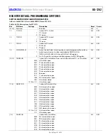
The high speed DAC transfer function is shown in Figure 25. Note that in Figure 26 the common-mode voltage setting for the calibration
circuit is set by the noninverting input of the high speed TIA.
RCAL0
+
HPTIA
–
RCAL1
EXCITATION
AMP
D
P
N
+
–
HIGH SPEED
DAC
N NODE
ADC
MUX
P NODE
N NODE
TO ADC
MUX
ADCVBIAS_CAP (1.11V)
VZERO0
VZERO1
HSTIACON[1:0]
VREF_1.8V
1.0V
0.2V
RCF
f
C
= 50kHz/100kHz/
250kHz
PMBW[3:2]
PGA
G = 1 OR 0.25
HSDACCON[12]
DAC
CLK
HSDACCON[0]
PMBW[0]
DACOFFSET
0
1
0
1
DACOFFSETHP
0
1
PMBW[0]
DACOFFSETATTEN
DACOFFSETATTENHP
DACGAIN
HSDACDAT[11:0]
SETS
COMMON-MODE
VOLTAGE
ADC MEASURES
DIFFERENTIAL VOLTAGE
BETWEEN P AND N NODES
TO CALIBRATE DAC
G = 2 OR G = 0.2
HSDACCON[0] (ATTENEN)
×
+
16
675
-12
9
Figure 26. High Speed DAC Calibration Circuit Using R
CAL
The example functions provided in the
kit demonstrate how to use the ADC to measure the differential voltage
across R
CAL
and how to adjust the appropriate offset calibration resistor until this differential voltage is approximately 0 V.
Table 127 shows the appropriate calibration for each high speed DAC output setting and the selected power mode of the analog die.
Table 127. High Speed Calibration Register Assignment for Each Output Range
HSDACCON,
Bit 12 Setting
HSDACCON,
Bit 0 Setting
Typical Output Range
(Code 0x200 to Code 0xE00)
Relevant Calibration Registers
Low Power Mode
High Power Mode
Low Power Mode/
High Power Mode
0 0 ±607
mV
DACOFFSET
DACOFFSETHP
DACGAIN
1 0 ±75
mV
DACOFFSET
DACOFFSETHP
DACGAIN
1 1 ±15.14
mV
DACOFFSETATTEN DACOFFSETATTENHP DACGAIN
0 1 ±121.2
mV
DACOFFSETATTEN DACOFFSETATTENHP DACGAIN


