ADM1060
Rev. B | Page 42 of 52
EEPROM
The ADM1060 has 512 bytes of nonvolatile, electrically erasable
programmable read-only memory (EEPROM) from register
addresses 0xF800 to 0xF9FF. This may be used for permanent
storage of data that will not be lost when the ADM1060 is pow-
ered down, unlike the data in the volatile registers. Although
referred to as read-only memory, the EEPROM can be written
to (as well as read from) via the serial bus in exactly the same
way as the other registers. The only major differences between
the EEPROM and other registers are
1. An EEPROM location must be blank before it can be written
to. If it contains data, it must first be erased.
2. Writing to EEPROM is slower than writing to RAM.
3. Writing to the EEPROM should be restricted because it has a
limited write/cycle life of typically 10,000 write operations,
due to the usual EEPROM wear-out mechanisms.
The EEPROM is split into 16 (0 to 15) pages of 32 bytes each.
Pages 0 to 6, starting at address 0xF800, hold the configuration
data for the applications on the ADM1060 (the PLB, SFDs, GPIs,
WDI, PDOs, etc.). These EEPROM addresses are the same as
the RAM register addresses, prefixed by 0xF8. Page 7 is
reserved. Pages 8 to 15 are for customer use. Data can be
downloaded from EEPROM to RAM in one of two ways:
1.
At power-up, pages 0 to 6 are downloaded.
2.
Setting Bit 2 of the UPDCFG register (0x90) performs a user
download of pages 0 to 6.
SERIAL BUS INTERFACE
Control of the ADM1060 is carried out via the serial system
management bus (SMBus). The ADM1060 is connected to this
bus as a slave device under the control of a master device. It
takes approximately 2 ms after power-up for the ADM1060 to
download from its EEPROM. Therefore, access to the
ADM1060 is restricted until the download is completed.
IDENTIFYING THE ADM1060 ON THE SMBus
The ADM1060 has a 7-bit serial bus slave address. When the
device is powered up, it will do so with a default serial bus
address. The five MSBs of the address are set to 10101, and the
two LSBs are determined by the logical states of Pins A1 and A0.
This allows the connection of four ADM1060s to the one
SMBus. The device also has a number of identification registers
(read only) that can be read across the SMBus. These are
Name Address Value Function
MANID 0x93
0x41
Manufacturer ID for Analog Devices
DEVID
0x94
0x3E
Device ID
REVID
0x95
0x– –
Silicon Revision
MARK1 0x96
0x– –
S/W Brand
MARK2 0x97
0x– –
S/W Brand
GENERAL SMBus TIMING
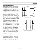
Figure 25 and Figure 26 show timing diagrams for general read
and write operations using the SMBus. The SMBus specification
defines specific conditions for different types of read and write
operation, which are discussed later. The general SMBus proto-
col operates as follows:
1. The master initiates data transfer by establishing a START condi-
tion, defined as a high-to-low transition on the serial data line
SDA while the serial clock line SCL remains high. This indicates
that a data stream will follow. All slave peripherals connected to
the serial bus respond to the START condition and shift in the
next eight bits, consisting of a 7-bit slave address (MSB first) plus
a R/W bit, which determines the direction of the data transfer,
i.e., whether data will be written to or read from the slave device
(0 = write, 1 = read).
The peripheral whose address corresponds to the transmitted
address responds by pulling the data line low during the low
period before the ninth clock pulse, known as the acknowl-
edge bit, and holding it low during the high period of this
clock pulse. All other devices on the bus now remain idle
while the selected device waits for data to be read from or
written to it. If the R/W bit is a 0, the master will write to the
slave device. If the R/W bit is a 1, the master will read from
the slave device.
2. Data is sent over the serial bus in sequences of nine clock pulses,
eight bits of data followed by an acknowledge bit from the slave
device. Data transitions on the data line must occur during the
low period of the clock signal and remain stable during the high
period, as a low-to-high transition when the clock is high may be
interpreted as a STOP signal.
If the operation is a write operation, the first data byte after
the slave address is a command byte. This tells the slave
device what to expect next. It may be an instruction such as
telling the slave device to expect a block write, or it may
simply be a register address that tells the slave where
subsequent data is to be written.
Since data can flow in only one direction as defined by the
R/W bit, it is not possible to send a command to a slave
device during a read operation. Before doing a read
operation, it may first be necessary to do a write operation to
tell the slave what sort of read operation to expect and/or the
address from which data is to be read.
3. When all data bytes have been read or written, stop condi-
tions are established. In WRITE mode, the master will pull
the data line high during the 10
th
clock pulse to assert a STOP
condition. In READ mode, the master device will release the
SDA line during the low period before the ninth clock pulse,
but the slave device will not pull it low. This is known as No
Acknowledge. The master will then take the data line low
during the low period before the 10
th
clock pulse, then high
during the 10
th
clock pulse to assert a STOP condition.

