ADM1060
Rev. B | Page 49 of 52
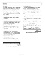
PIN CONFIGURATION AND FUNCTIONAL DESCRIPTIONS
28
27
26
25
24
23
22
21
20
19
18
17
16
15
1
2
3
4
5
6
7
8
9
10
11
12
13
14
ADM1060
VB2
VB1
VP4
VP3
VP2
VP1
VH
A0
A1
SDA
SCL
VCCP
GND
VDDCAP
PDO1
PDO2
PDO3
PDO4
PDO5
PDO6
PDO7
GPI1
GPI2
GPI3
GPI4
PDO8
PDO9
WDI
TOP VIEW
(Not to Scale)
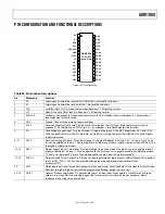
Figure 38. Pin Configuration
Table 58. Pin Function Descriptions
Pin Mnemonic Function
1
A0
Logic Input. Controls the seventh bit (LSB) of the 7-bit Serial Bus Address.
2
A1
Logic Input. Controls the sixth bit of the 7-bit Serial Bus Address.
3
SDA
Serial Bus Data I/O Pin. Open-Drain output. Requires 2.2 kΩ pull-up resistor.
4
SCL
Open-Drain Serial Bus Clock Pin. Requires 2.2 kΩ pull-up resistor.
5 VDDCAP V
DD
Bypass Capacitor Pin. A capacitor from this pin to GND stabilizes the V
DD
Arbitrator. A 1 µF capacitor is
recommended for this function.
6
GND
Ground. Connect to common of power supplies.
7 VCCP
Reservoir Capacitor for Central Charge Pump. This provides the first stage in the tripler circuits used to
produce 12 V of gate drive on PDOs 1 to 4. A 1 µF capacitor is recommended for this function.
8 VH
High Voltage Supply Input. Two input ranges. A supply of between 2 V and 6 V or between 4.8 V and 14.4 V
can be applied to this pin. The V
DD
arbitrator will select this supply to power the ADM1060 if it is the highest
supply supervised.
9–12 VP1–4
Positive Only Supply Inputs. Three input ranges. A supply of between 0.6 V and 1.8 V, 1 V and 3 V, or 2 V and
6 V can be applied to this pin. The V
DD
arbitrator will select one of these supplies to power the ADM1060 if it is
the highest supply supervised.
13–14 VB1–2
Bipolar Supply Inputs. Two modes. Two input ranges in positive mode. One input range in negative mode. A
supply of between –6 V and –2 V can be applied to this pin when set in negative mode. A supply of between
1 V and 3 V or between 2 V and 6 V can be applied to this pin when set in positive mode.
15–23 PDO1–9
Programmable Driver Output Pin. All nine can be programmed as logic outputs with multiple pull-up options
to V
DD
or VPn. PDOs 1 to 4 can also provide a charge-pump generated gate drive for external
N-channel FETs.
24 WDI
Watchdog Input. Used to monitor a processor clock and asserts a fault condition if the clock fails to transition
from low-to-high or high-to-low within a programmed timeout period (up to 18 sec).
25–28 GPI4–1
General-Purpose Logic Input. TTL compatible logic. Can be used as, for example, a manual reset, a chip en-
able pin, or an input for a control logic signal that may be used to initiate the power-up/power-down
sequence of the supplies under control.

