background image

ADAR1000-EVALZ

 User Guide 

UG-1283


Rev. A | Page 13 of 24 

QUICK TEST PROCEDURE 

To use the ADAR1000-EVALZ to test and evaluate the 

ADAR1000

, take the following steps: 

1.


Plug the SDP adapter into the P5 connector on the 
ADAR1000-EVALZ. 

2.


Connect the 3.3 V and −5 V power supplies to the 
corresponding banana jacks on the ADAR1000-EVALZ. 

3.


Use a USB cable to connect the SDP adapter to the PC that 
has the ADAR1000-EVALZ evaluation software downloaded. 

4.


Connect one port of the network analyzer to the RF_IO 
connector and another port to the RX1 input connector. 

5.


Use the 

Start

 menu to run the ADAR1000-EVALZ 

evaluation software (see the Evaluation Board Software 
Installation s
ection for more information), as shown in 
Figure 24. 

16

78

8-

10

6


Figure 24. Run Control Software from the 

Start

 Menu 

6.


After the ADAR1000-EVALZ evaluation software starts up, 
click the 

Connection

 tab and then click 

Connect

 (see 

Figure 27). 

7.


Ensure that 

SDP board connected

 appears on the status bar. 

8.


For receive mode operation, click the 

Manual Register 

Write

 tab (see Figure 21) and click 

Choose Input File

 to 

choose the 

RX1_MaxG_45.txt

 file for the register values. 

Note that this file (and the similar settings files) does not 
change any of the GUI settings. The file only writes data to 
the 

ADAR1000

.  

9.


Click 

Write All

 to send the register values to th

ADAR1000

Receive Channel 1 is now turned on at full gain. 

10.


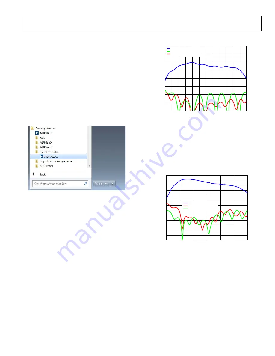
Measure the gain and return loss on the network analyzer. A 
typical response is shown in Figure 25. 

20

6

7

8

9

10

11

12

FREQUENCY (GHz)

13

14

15

16

17

18

15

10

5

0

G

AI

N

A

ND RE

T

URN L

O

SSES (

d

B

)

–5

–10

–15

–20

MEASURED GAIN
RX1 RETURN LOSS
RF_IO RETURN LOSS

167

88-

0

04


Figure 25. Receive Mode Gain and Return Loss Measurement Results  

11.


For transmit mode operation, disconnect the RX1 port and 
connect to the TX1 output connector. 

12.


Click 

Choose Input File 

to choose the 

TX1_MaxG_45.txt


file for the register values. 

13.


Click 

Write All

 to send the register values to th

ADAR1000

Transmit Channel 1 is now turned on at full gain. 

14.


Measure the gain and return loss on the network analyzer. A 
typical response is shown in Figure 26. 

25

20

–40

–35

–30

–25

–20

–15

–10

–5

0

5

10

15

6

18

16

14

12

10

8

G

AI

N AND RE

T

URN 

L

O

S

S

 (

d

B)

FREQUENCY (GHz)

GAIN
RETURN LOSS TXx
RETURN LOSS RF_IO

16

78

8-

22

6


Figure 26. Transmit Mode Gain and Return Loss  


Summary of Contents for ADAR1000-EVALZ

Page 1: ...ting the performance of the ADAR1000 4 channel X band and Ku band beamformer for radar systems All radio frequency RF input output channels and detector inputs are brought out to Subminiature Version A SMA connectors On board logic level translators convert the on chip 1 8 V logic signals to 3 3 V for interfacing to external controllers running on 3 3 V Two identical 20 pin dual row rectangular he...

Page 2: ...Module Compatible Interface Section 5 Added Transmit and Receive Startup Using the GUI Section Resetting the Registers Changing to a 4 Wire SPI and Setting the LDO Voltage Section Figure 6 Transmit Startup Section Bypassing the RAM Section Figure 7 Enabling Transmit Channels Section and Figure 8 Renumbered Sequentially 8 Added Setting Transmit Bias Currents Section SPI Control and Enabling Transmi...

Page 3: ...shown in Figure 2 POWER SUPPLY REQUIREMENTS The ADAR1000 EVALZ is powered via two external supplies see Table 1 Connections to the ADAR1000 EVALZ are described in the Quick Test Procedure section Note that the 3 3 V banana jack has no function and therefore is not populated Table 1 External Supply Details Pin Supply Board Label Capacity AVDD3 3 3 3 3 V 600 mA AVDD1 5V 5 0 V 50 mA RADIO FREQUENCY I...

Page 4: ... tied together through the daisy chain Pin 15 on P1 and P2 by installing a 0 Ω resistor jumper R36 The pinout of P1 and P2 is shown in Table 3 The TR TX_LOAD RX_LOAD and PA_ON pins on the ADAR1000 are also controlled by software via general purpose input output GPIO lines on the SDP connector and 3 3 V to 1 8 V level shifters Table 3 Digital Interface Connectors P1 and P2 Pinout Pin1 Signal Name F...

Page 5: ...high Position 3 Not Connected AD1 low Position 2 to Position 4 AD0 is controlled by SDP GPIO3 Position 4 to Position 6 AD0 high Position 4 Not Connected AD0 low Peripheral Module Compatible Interface The 3 3 V digital interface signals are also repeated on Connector P3 arranged to be compatible with the peripheral module interface connector available on many field programmable gate array FPGA eval...

Page 6: ...corresponding own bias output Table 8 Transmit and Receive Module Interface Signal Descriptions Signal Description TR_SW_NEG 0 V to 5 V output to drive an external transmit and receive switch TR_SW_POS 0 V to 3 3 V output to drive an external transmit and receive switch TR_POL 0 V to 5 V output to drive an external antenna polarization switch LNA_BIAS Provides a common bias control voltage 0 V to ...

Page 7: ...ate to that location using the File Manager and double click the file name to open it 16788 104 Figure 4 Saving Downloaded Control Software Zip File 3 The File Manager shows the content of the zip file as shown in Figure 5 16788 105 Figure 5 Unpacking Software Zip File 4 Double click the EV ADAR1000_2p1p0 exe file to start the installation Click Yes when asked to allow the program to make modifica...

Page 8: ...ister Write tab either all at once in the Load and Write section or individually in the Values to write section see Figure 6 16788 206 Figure 6 Using the Load and Write Feature to Perform Several Writes When all values are loaded via a txt file or typed manually click Write All to write the data to the device TRANSMIT STARTUP When powering up the device or after performing a soft reset the ADAR100...

Page 9: ...Write Switch Note that leaving the TR SOURCE check box cleared places the device in SPI control mode which is the default mode 16788 210 Figure 10 SPI Control Transmit Enable and Transmit Mode Transmit Gain Control To set the transmit Channel 1 gain to maximum take the following steps 1 Click the TX Registers tab see Figure 11 2 Select the CH1 TX ATTN check box to bypass the attenuator on Channel ...

Page 10: ...Click the MISC tab see Figure 14 2 Select the BEAM RAM BYPASS check box and the BIAS RAM BYPASS check box 3 Click Write Value 16788 214 Figure 14 Placing the Device in RAM Bypass Mode Enabling Receive Channels To enable the receive channels and associated circuits take the following steps 1 Click the T R Control tab see Figure 15 2 Select all check boxes in the Rx Enable section to enable all four...

Page 11: ...eive Gain Control with All Other Channels at Minimum Gain Receive Phase Control To set Receive Channel 1 to 45 take the following steps 1 Click the RX Registers tab see Figure 19 2 Select the inphase I and quadrature phase Q check boxes under RX VM CH1 POL to set the polarity bits so that the vector is in the first quadrant 3 Set the I and Q values under RX VM CH1 GAIN to 22 for a resulting vector...

Page 12: ...put File 3 Navigate to where the settings files are located see Figure 22 4 Open the desired file Tx1_MaxG_45 txt for example 5 The values in the file appear in the larger text box on the left side of the window as shown in Figure 23 6 Click Write All to load all values via the SPI 16788 221 Figure 21 Manual Register Write Tab 16788 222 Figure 22 Choose Settings File 16788 223 Figure 23 Values to ...

Page 13: ...and click Choose Input File to choose the RX1_MaxG_45 txt file for the register values Note that this file and the similar settings files does not change any of the GUI settings The file only writes data to the ADAR1000 9 Click Write All to send the register values to the ADAR1000 Receive Channel 1 is now turned on at full gain 10 Measure the gain and return loss on the network analyzer A typical ...

Page 14: ... EVALZ hardware CONNECTION TAB The Connection tab displays the two different SDP adapters that can be used to provide the USB interface to the ADAR1000 EVALZ see Figure 27 Click the Connect button to initialize communication between the ADAR1000 EVALZ evaluation software and the ADAR1000 EVALZ When communication is established the SDP board connected message displays on the status line at the bott...

Page 15: ...l In the Tx Phase Control section set the I and Q gain registers as well as polarity bits for each channel in the corresponding vector modulator VM In the Memory Index section if the SPI Ctrl check box is selected the beam position settings for the corresponding channel are recalled from memory into the channel work registers according to the value the memory address in the TX CH1 RAM INDEX to TX ...

Page 16: ... each receive channel In the Rx Phase Control section set the I and Q gain registers for each channel in the corresponding VM In the Memory Index section if the SPI Ctrl check box is selected the beam position settings for the corresponding channel are recalled from memory into the channel work registers according to the value the memory address in the RX CH1 RAM INDEX to RX CH4 RAM INDEX field fo...

Page 17: ...x under Switch Control is selected the receive enable functions are enabled and the transmit enable functions are disabled When the check boxes are selected or cleared click Write Enable Values or Write Switch Values in each section to write the register settings to the ADAR1000 EVALZ GPIO TAB In the GPIO tab see Figure 33 select the correct check boxes to set the corresponding digital control sig...

Page 18: ...register values only If the BIAS CTRL check box is selected while the device is in receive mode the PA DACs use the Bias OFF register values and the LNA DAC uses the Bias ON register value If the check box is selected while the device is in transmit mode the opposite is true and the PA DACs use the Bias ON register values and the LNA DAC uses the Bias OFF register values In the ADC section use the...

Page 19: ...ry address is the four most significant digits and the data for each memory location is the two least significant digits Typical entries in a beam position file include the following 1573119 0x1800FF 1573174 0x180136 1573429 0x180235 The starting and ending memory locations Start Point and End Point respectively as well as the time delay between steps Time Delay ms is entered into the correspondin...

Page 20: ...0 EVALZ When the device is initially powered up enter 00099 into the Values to write section Entering 00099 performs a full register reset and enables the 4 wire SPI SDO function READBACK TAB The ReadBack tab allows direct writing and reading of the content of a register see Figure 38 Click Manual Write to write a string of hexadecimal digits containing the address and data of a register into the ...

Page 21: ... 3 8 4 10 16 14 12 0 0 200 200 0 0 LNA_B1 TR_SW_POS PA_B4 22 1K TR_POL LNA_B1 100PF C29 AVDD1 C24 C22 C26 C30 R6 22 1K 22 1K 22 1K R11 AVDD3 PA_B1 TR_SW_POS TR_SW_NEG PA_B2 200 200 R26 0 TX2 TBD0402 B8 B6 A6 M4 M3 M1 L13 J2 H2 H1 G1 D13 D2 D1 C2 B11 B10 B7 B4 A13 A4 H12 N1 A1 A3 A2 A5 A7 TR_SW_NEG PA_B3 R9 A10 0 TR_POL TR_POL 200 24 R35 22 R22 B5 TR_SW_POS PA_B3 TR_SW_NEG TR_SW_POS 200 R34 23 B2 B...

Page 22: ... 18 13 12 9 8 7 4 3 2 1 6 18 17 16 15 14 13 12 10 9 8 7 6 5 4 3 2 1 AVDD SPI_MISO SPI_CLK GPIO5 GPIO1 SPI_MOSI VIO GPIO4 GPIO2 GPIO0 DVDD DVDD GPIO5 AVDD PA_ON AVDD AVDD 10PF P3 0 6 17 16 GPIO0 1 10K 10PF 1 2 P4 1 12 AVDD C11 14 6 2 SDO 24LC32A I MS GPIO3 SPI_SEL_A 118 12 13 69157 102HLF 2 5 0 TR 7 0 8 TX_LOAD 6 7 11 15 14 0 10 AD1 1 0 1UF 4 C12 69157 102HLF AVDD C1 AVDD AVDD2 AVDD1 GPIO0 GPIO4 GP...

Page 23: ...ADAR1000 EVALZ User Guide UG 1283 Rev A Page 23 of 24 16788 019 Figure 41 Layer 1 Component Side 16788 020 Figure 42 Layer 4 Bottom Side ...

Page 24: ...party for any reason Upon discontinuation of use of the Evaluation Board or termination of this Agreement Customer agrees to promptly return the Evaluation Board to ADI ADDITIONAL RESTRICTIONS Customer may not disassemble decompile or reverse engineer chips on the Evaluation Board Customer shall inform ADI of any occurred damages or any modifications or alterations it makes to the Evaluation Board...

Reviews: