background image

Evaluation Board User Guide 

UG-076


Rev. A | Page 5 of 16 

QUICK START GUIDE TO THE 

AD9520

 PLL 

When the evaluation software is installed, the evaluation board 
is connected, and the software is loaded, use the following steps 
to configure and lock the PLL. These steps assume that the input 
signal is present, the evaluation board has not been modified, 
and that the PLL loop filter is suitable for the user’s application. 

This quick start guide covers only simple PLL operation to start 
the PLL. See th

AD9520

 data sheet and Evaluation Software 

Components section for a detailed explanation of the various 

AD9520

 features. 

The following case is an example for th

AD9520-4

 using the 

values in Table 1. 

Table 1. Default Parameter Values 

Parameter Value 

Input Frequency 

19.44 MHz on REF1 

Output Frequency 

148.5 MHz 

Reference Divider 

72 

Phase Detector Frequency 

270 kHz 

Feedback Divider 

5500 

VCO Frequency 

1485 MHz 

VCO Divider 

Channel Divider 

1.


Turn the PLL on by selecting 

Normal Op

 from the 

PLL 

MODE

 box found at the top of the main window (see 

Figure 8)

2.


Enter the intended reference input frequency (in 
megahertz) in the 

REF 1 (MHz)

 box at the upper left 

corner of the main window. 

3.


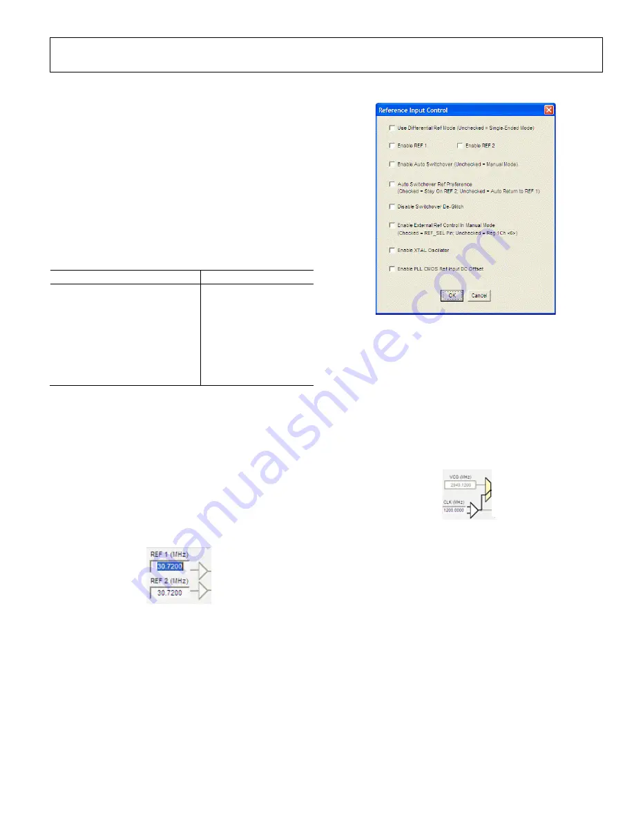
Click the triangular buffer symbol immediately to the  
right of the input reference frequency text boxes (see 
Figure 4) to open the 

Reference Input Control

 window 

shown in Figure 5. Turn the REF1 reference input buffer on 
by selecting the 

Enable REF 1

 check box, and then click 

OK

.  

0

874

6-

024


Figure 4. Buffer Symbol 


08

74

6-

0

04


Figure 5. 

Reference Input Control

 Window 

4.


When the window closes, the 

WRITE

 button under the 

REGISTER W/R

 section in Figure 8 blinks red. This 

indicates that there are settings that have not been loaded 
to th

AD9520

 evaluation board. Click the blinking red 

WRITE

 button to load these settings to the evaluation 

board. 

5.


Select the VCO as the input to the clock distribution 
circuitry by clicking the mux symbol that is located 
immediately to the right of the 

VCO (MHz)

 box (see 

Figure 6).  

0

874

6-

025


Figure 6. Mux Symbol 

6.


When the VCO is selected, the border of the 

VCO (MHz)


box changes from gray to black. The current VCO 
frequency is shown in the 

VCO (MHz)

 box. 

Summary of Contents for AD9520-0

Page 1: ...are very low noise phase locked loop PLL clock synthesizers featuring an integrated voltage controlled oscillator VCO clock dividers and up to 24 outputs The AD9520 product series features automatic...

Page 2: ...D9520 on a User Board 15 AD9520 Binary File Generation 16 Checksum Generation 16 Avoiding Checksum Mismatches 16 REVISION HISTORY 5 2017 Rev 0 to Rev A Changes to Title and General Description Section...

Page 3: ...ng is recommended in applications requiring automatic hitless reference switching There is a possibility that the AD9520 receive buffer can chatter when an ac coupled clock stops toggling Connect an o...

Page 4: ...ing that the evaluation board was found or red text appears indicating that the evaluation board was not found 2 If the evaluation board is found click anywhere in the pop up window with the Evaluatio...

Page 5: ...p from the PLL MODE box found at the top of the main window see Figure 8 2 Enter the intended reference input frequency in megahertz in the REF 1 MHz box at the upper left corner of the main window 3...

Page 6: ...f the CHARGE PUMP box However this setting normally does not need to be modified 11 Set the VCO divider by clicking the green VCO box in the center of the main window immediately to the left of the Ca...

Page 7: ...are listed in the following sections and each of these subsections has its own window From the main window each functional block can be accessed by clicking that block in the main window When a subwi...

Page 8: ...N WINDOW The PLL Configuration window shown in Figure 11 is opened by clicking the Config PLL button on the main screen The window has three sections SyncB Counter Reset Mode PLL Status Registers and...

Page 9: ...ssed by clicking the EEPROM button near the lower left corner of the main window 08746 008 Figure 12 EEPROM Control Window To store the current register settings of the AD9520 to the EEPROM click the...

Page 10: ...der value For example it is not possible to use the internal VCO and a feedback divider of 30 However the R divider can be doubled which allows a feedback divider of 60 The feedback divider window has...

Page 11: ...king the Cal VCO button in the main window 08746 015 Figure 19 Calibrate VCO Window A valid reference input signal must be present to complete VCO calibration and the VCO must be recalibrated any time...

Page 12: ...istors on each output This termination scheme is ideal for LVPECL drivers However this scheme degrades the CMOS driver performance Improved CMOS driver performance is achieved by removing the 200 pull...

Page 13: ...ted evaluation board see Figure 25 08746 019 Figure 25 Select USB Device Window Configure Serial Port The I O Interface window allows the user to control how the USB controller interacts with the AD95...

Page 14: ...better choice Typical phase detector frequencies for these applications are 10 MHz to 100 MHz and typical loop bandwidths for this loop filter are 50 kHz to 500 kHz depending on the configuration The...

Page 15: ...and then click Detect Current Configuration A dialog box appears and acknowledges the I2 C mode and address The evaluation software starts at I2 C Address 0x058 and stops at the first valid I2 C addre...

Page 16: ...MA 02062 USA Subject to the terms and conditions of the Agreement ADI hereby grants to Customer a free limited personal temporary non exclusive non sublicensable non transferable license to use the Ev...

Reviews: