background image

CoreModule 420

Reference Manual

1

Chapter 1

About This Manual

Purpose of this Manual

This manual is for designers of systems based on the CoreModule™ 420 PC/104 single board computer
(SBC) module.  This manual contains information that permits designers to create an embedded system
based on specific design requirements.

Information provided

 in this reference manual includes:

CoreModule 420 SBC Specifications

Environmental requirements

Major chips and features implemented

CoreModule 420 SBC connector/pin numbers and definition

BIOS Setup information

Information not provided

 in this reference manual includes:

Detailed chip specifications

Internal component operation

Internal registers or signal operations

Bus or signal timing for industry standard busses and signals

Reference Material

The following list of reference materials may be helpful for you to complete your custom design
successfully.  Most of this reference material is also available on the Ampro web site in the Embedded
Design Resource Center.  The Embedded Design Resource Center was created for embedded system
developers to share Ampro’s knowledge, insight, and expertise gained from years of experience.

Specifications

PC/104 Specifications Revision 2.5, November 2003.

For latest revision of the PC/104 specifications, contact the PC/104 Consortium, at:

Web site: 

http://www.pc104.org

Chip Specifications

The following chip specifications are used in the CoreModule 420 processor module:

STMicroelectronics and the chip, STPC

®

 Atlas, used for the embedded CPU

Web site: 

http://us.st.com/stonline/books/pdf/docs/7341.pdf

Standard Microsystems Corp and the chip, FDC37B782, used for the Super I/O controller

Web site: 

http://www.smsc.com/main/catalog/fdc37b78x.html

Intel Corporation and the chip, 82551ER, used for the Ethernet controller

Web site: 

http://www.intel.com/design/network/products/lan/controllers/82551er.html

Summary of Contents for CoreModule 420

Page 1: ...CoreModule 420 PC 104 Single Board Computer Reference Manual P N 5001692A Revision A ...

Page 2: ...eserves the right to revise this publication from time to time without obligation to notify any person of such revisions If errors are found please contact Ampro at the address listed below on the Notice page of this document TRADEMARKS Ampro and the Ampro logo are registered trademarks and CoreModule EnCore Little Board LittleBoard MiniModule and ReadyBoard are trademarks of Ampro Computers Inc A...

Page 3: ...cal Specifications 14 Power Specifications 15 Environmental Specifications 15 Thermal Cooling Requirements 15 Chapter 3 Hardware 17 Overview 17 CPU U14 18 Memory 18 SDRAM Memory U7 U8 U9 U10 18 Flash Memory U6 18 Bytewide Socket U5 18 Memory Map 18 Interrupt Channel Assignments 20 I O Address Map 20 PC 104 Bus Interface P1A B C D 22 IDE Interface J6 27 CompactFlash Socket J12 29 Floppy Parallel Po...

Page 4: ... B Connector Part Numbers 59 Index 61 List of Figures Figure 2 1 Stacking PC 104 Modules with the CoreModule 420 5 Figure 2 2 CoreModule 420 Block Diagram 9 Figure 2 3 CoreModule 420 Top View 10 Figure 2 4 Connector Locations Top View 11 Figure 2 5 Jumper and LED Locations Top View 13 Figure 2 6 Connector Location Bottom View 13 Figure 2 7 Mechanical Dimensions Top View 14 Figure 3 1 Serial 1 to R...

Page 5: ...ons J12 29 Table 3 11 Parallel Interface SPP Pin Signal Descriptions J4 31 Table 3 12 Serial Ports Pin Signal Descriptions J3 J9 34 Table 3 13 Serial 3 4 Interface Pins Signals J13 J14 34 Table 3 14 USB Interface Pin and Signal Designations J10 35 Table 3 15 Utility Interface Pin Signal Descriptions J5 36 Table 3 16 Ethernet Interface Pin Signal Descriptions J2 37 Table 3 17 Video Interface Pin Si...

Page 6: ...Contents vi Reference Manual CoreModule 420 ...

Page 7: ...ay be helpful for you to complete your custom design successfully Most of this reference material is also available on the Ampro web site in the Embedded Design Resource Center The Embedded Design Resource Center was created for embedded system developers to share Ampro s knowledge insight and expertise gained from years of experience Specifications PC 104 Specifications Revision 2 5 November 2003...

Page 8: ...ivers Other CoreModule Products CoreModule 410 This PC 104 embedded CPU is a state of the art high integration x86 based computer using STMicroelectronics 133MHz STPC Elite processor which provides a complete embedded PC solution with most of the standard peripheral interfaces In addition to the standard CoreModule features PC 104 form factor PC 104 bus 5 volt power etc it includes 16MB soldered S...

Page 9: ... PC Card expansion analog data acquisition FPGA additional RS232 RS485 serial ports and general purpose I O GPIO EnCore Family These high performance compact modular CPU solutions use various processor technologies including Intel x86 MIPS and PowerPC architectures to plug into your custom logic board Each EnCore module provides standard peripherals including IDE floppy drive interface PCI bus ser...

Page 10: ...Chapter 1 About this Manual 4 Reference Manual CoreModule 420 ...

Page 11: ... PCMCIA interfaces Sound cards PC 104 expansion modules can be stacked with the CoreModule 420 avoiding the need for card cages and backplanes The PC 104 expansion modules can be mounted directly to the PC 104 bus connector of the CoreModule 420 PC 104 compliant modules can be stacked with an inter board spacing of 0 66 inches so that a 3 module system fits in a 3 6 inch by 3 8 inch by 2 4 inch sp...

Page 12: ...y well suited to either embedded or portable applications Its flexibility makes system design quick and easy It can be stacked with Ampro MiniModules or other PC 104 compliant expansion or it can be used as the computing engine in a fully customized application Module Features CPU Supports 133MHz x86 based STPC ATLAS microprocessor Fully PC compatible architecture 8kB Unified Instruction and Data ...

Page 13: ...llel Port Shared connector with Floppy drive port Supports standard printer port Supports IEEE standard 1284 protocols including EPP ECP modes Bidirectional data lines Supports 16 byte FIFO for ECP mode Ethernet Controller Intel 82551ER Controller chip Supports IEEE 802 3 10BaseT 100BaseT compatible physical layer Supports Auto negotiation for speed duplex mode and flow control Supports full duple...

Page 14: ...upports video memory up to 4MB selected in BIOS Setup CRT VGA Controller with 135MHz triple RAMDACs for 1280 x 1024 x 75Hz display Supports 24 bit pixel depth Interlaced or non interlaced output LCD TFT Controller Supports VESA Flat Panel Display interface FPDI 1B Supports programmable panel size up to 1024x768 pixel display resolution Supports VGA and SVGA active matrix TFT flat panels Support in...

Page 15: ...D CompactFlash CD ROM etc Ethernet Controller Memory SDRAM CPU Core Host Peripheral Interface Super I O Controller Floppy Drive BIOS Internal PCI Bus Parallel Port PC 104 Interface DiskOnChip ISA Bus Utility Interface Keyboard Mouse External Bat etc Video CRT TFT RTC Serial Ports Serial 3 4 Serial Ports Serial 1 2 USB Port I C Interface 2 CM420blkdiag Figure 2 2 CoreModule 420 Block Diagram ...

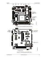
Page 16: ...ller I O features and power management capabilities Embedded CPU Super I O Controller U13 Standard Microsystems Corp FDC37B782 Super I O This chip provides serial and Floppy controllers Floppy Serial Controllers Ethernet Controller U15 Intel 82551ER Ethernet This chip provides the 10 100BaseT Ethernet function Ethernet U5 J3 JP2 J4 U6 U15 U16 D1 D2 U14 U8 U7 U9 U10 J8 JP7 JP8 JP9 JP6 U36 U35 U3 U4...

Page 17: ...tor used for the Power connection J8 GPIO User Top 10 pin 2mm connector used for the User defined GPIO signals J9 Serial 2 COM2 Top 10 pin 0 1 connector used for the Serial 2 interface J10 USB Top 5 pin 0 1 connector used for the USB interface J11 Video Top 44 pin 2mm connector used for the LCD CRT interface J12 CompactFlash Bottom 50 pin connector used for CompactFlash cards J13 Serial 3 COM3 Top...

Page 18: ...000h DDFFFh Pins 1 2 Access from CC000h CDFFFh No jumper JP8 Serial Port 1 Enable Serial Port 1 Pins 1 2 Default setting Disabled Serial Port 1 Pins 2 3 JP9 Serial Port 2 Enable Serial Port 2 Pins 1 2 Default setting Disabled Serial Port 2 Pins 2 3 Note JP8 and JP9 Enable Disable the Serial ports at the STPC Altas CPU U14 LED Definitions Table 2 4 provides the LED color and definitions for the Eth...

Page 19: ... JP4 JP5 9 10 10 2 4 3 1 1 2 1 2 JP1 JP2 Link Activity LED D1 Speed LED D2 JP6 JP9 Bytewide Socket U5 Pin 1 JP4 JP5 JP8 JP7 JP1 CM420RFM_01c Figure 2 5 Jumper and LED Locations Top View D5 U21 U42 Y2 Y3 Y1 U29 U25 U38 U27 U30 U28 F1 J12 U23 U24 U19 U1 D3 D4 U37 U20 U22 CompactFlash Socket J12 PC 104 Bus P1 USB Fuse F1 Voltage Regulator U19 CM420RFM_02a Figure 2 6 Connector Location Bottom View ...

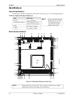
Page 20: ...of the board to the highest permanent component on the upper surface of the board Mechanical Specifications J9 J6 J11 J10 J7 J2 J4 J3 J5 P1B P1A P1C P1D JP2 J8 JP7 JP8 JP9 JP6 J13 J14 JP4 JP5 9 10 10 4 3 1 2 1 2 JP1 0 000 0 000 0 300 0 200 0 700 0 940 2 890 3 375 3 575 3 431 0 150 0 400 2 375 3 050 2 500 0 394 0 850 3 190 3 105 3 375 3 400 3 350 0 280 0 030 0 020 0 050 0 000 0 000 0 010 0 200 3 11...

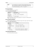
Page 21: ...s Input Voltage Requirements 5 VDC 5 1 35 Amps typical Operating Power 6 75 Watts typical Note Current readings were taken with all peripheral devices connected or simulated using the Windows 2000 operating system Environmental Specifications Table 2 7 provides the most efficient operating and storage condition ranges required for this module Table 2 7 Environmental Requirements Parameter Conditio...

Page 22: ...Chapter 2 Product Overview 16 Reference Manual CoreModule 420 ...

Page 23: ...board Mouse Battery Reset Switch Speaker Ethernet J2 USB J10 Video J11 Miscellaneous Time of Day RTC User GPIO J8 Oops Jumper BIOS Recovery Watchdog timer Power J7 NOTE Ampro Computers Inc only supports the features options tested and listed in this manual The main integrated circuits chips used in the CoreModule 420 may provide more features or options than are listed for the CoreModule 420 but s...

Page 24: ...to place on the module and operating at 100MHz Flash Memory U6 A 1MB flash device is used for system BIOS on the module and 768kB is available for user code The Flash memory also stores system parameters CMOS settings for battery less boot capability when no battery is available Bytewide Socket U5 The CoreModule 420 has a 32 pin DIP socket on the module used as a bytewide memory socket This socket...

Page 25: ...H R R 00E0 0000 1MB H H R R R 00D0 0000 1MB H H R R R 00C0 0000 1MB H R R R R 00B0 0000 1MB H R R R R 00A0 0000 1MB H R R R R 0090 0000 1MB H R R R R R RAM H Memory Hole forwarded to ISA The board can be configured to have access to the 1MB Flash anywhere in the memory hole on 1MB alignment 0080 0000 7MB RAM 0010 0000 128kB Shadowed BIOS 000E 0000 8kB Unused 000D E000 8kB DiskOnChip if DC000 DDFFF...

Page 26: ... IDE D Z Sec IDE D Z USB O O O O O O O O O D O Z Ethernet O O O D O O O O O O O Z Math Coprocessor X PS 2 Mouse O O O O O O O O O D Z Legend D Default O Optional X Fixed Z Disable option NOTE The devices listed with a Z in the Disable column indicate the device can be disabled which will free the IRQ for another device in the list Table 3 3 DMA Map DMA Use 0 1 5 6 7 2 Floppy configurable 3 LPT 1 o...

Page 27: ...e mode only 03C0 03CF VGA registers 03D4 03D5 VGA registers color mode only 03DA VGA registers color mode only 03E8 03EF COM3 configurable 03F0 03F1 Super I O Configuration 03F0 03F5 Floppy Disk Controller configurable 03F6 Primary IDE see 1F0 03F7 Floppy Disk Controller see 3F0 03F8 03FF COM1 configurable 0778 077A LPT 1 only in ECP modes 0CF8 PCI Configuration Address 0CFC 0CFF PCI Configuration...

Page 28: ...s drive the signal inactive low not ready to insert wait states Devices using this signal to insert wait states should drive it low immediately after detecting a valid address decode and an active read or write command The signal is released high when the device is ready to complete the cycle 11 A11 AEn Address Enable This signal is reserved for the ISA Bus and is asserted during DMA cycles to pre...

Page 29: ...iven low by a bus slave device to indicate it is capable of performing a bus cycle without inserting any additional wait states To perform a 16 bit memory cycle without wait states this signal is derived from an address decode 41 B9 12V 12 Volts 42 B10 Key NC Key Pin Not connected 43 B11 SMemW System Memory Write This signal is used by bus owner to request a memory device to store data currently o...

Page 30: ...t 3 Asserted by a device when it has pending interrupt request Only one device may use the request line at a time 58 B26 DAck2 DMA Acknowledge 2 Used by DMA controller to select the I O resource requesting the bus or to request ownership of the bus as a bus master device Can also be used by the ISA bus master to gain control of the bus from the DMA controller 59 B27 TC Terminal Count This signal i...

Page 31: ...ptions P1D Pin Signal Description P1 Row D 21 D0 GND Ground 22 D1 MCS16 Memory Chip Select 16 This is signal is driven low by a memory slave device to indicates it is cable of performing a 16 bit memory data transfer This signal is driven from a decode of the LA23 to LA17 address lines 23 D2 IOCS16 I O Chip Select 16 This signal is driven low by an I O slave device to indicate it is capable of per...

Page 32: ...st be held high until associated DACK6 line is active 35 D14 DAck7 DMA Acknowledge 7 Used by DMA controller to select the I O resource requesting the bus or to request ownership of the bus as a bus master device Can also be used by the ISA bus master to gain control of the bus from the DMA controller 36 D15 DRQ7 DMA Request 7 Used by I O resources to request DMA service Must be held high until ass...

Page 33: ... to pin 3 D7 for more information 9 D4 Disk Data 4 Refer to pin 3 D7 for more information 10 D11 Disk Data 11 Refer to pin 3 D7 for more information 11 D3 Disk Data 3 Refer to pin 3 D7 for more information 12 D12 Disk Data 12 Refer to pin 3 D7 for more information 13 D2 Disk Data 2 Refer to pin 3 D7 for more information 14 D13 Disk Data 13 Refer to pin 3 D7 for more information 15 D1 Disk Data 1 R...

Page 34: ...ted IRQ 14 by drive when it has pending interrupt request PIO transfer of data to or from the drive to the host 32 NC Not connected 33 LA18 Latch Address 18 Used to indicate which byte in the ATA command block or control block is being accessed 34 NC Not connected through 0 047 µf capacitor to ground 35 LA17 Latch Address 17 Used to indicate which byte in the ATA command block or control block is ...

Page 35: ...isk Data 5 Refer to pin 2 D3 for more information 5 D6 Disk Data 6 Refer to pin 2 D3 for more information 6 D7 Disk Data 7 Refer to pin 2 D3 for more information 7 CE1 Card Enable 1 This signal along with CE2 is used to select the card and indicate to the card when a byte or word operation is being performed This signal accesses the even byte or odd byte of the word depending on A0 and CE2 8 GND D...

Page 36: ...rs on the negative to positive edge of the signal trailing edge 36 Vcc 5 volts 5 power supply WE 37 RDY Drive Ready IRQ IRQ 14 is asserted by drive CF when it has a pending interrupt request PIO transfer of data to or from the drive to the host 38 Vcc 5 volts 5 power supply 39 GND Grounded CSEL 40 NC Not Connected VS2 41 IDERst IDE Reset This input signal is the active low hardware reset from the ...

Page 37: ...allel Port EPP and Enhanced Capabilities Port ECP protocols Table 3 11 Parallel Interface SPP Pin Signal Descriptions J4 Pin Signal Description 1 Strobe Strobe This is an output signal used to strobe data into the printer I O pin in ECP EPP mode 2 AutoFD DRVO Auto Feed This is a request signal into the printer to automatically feed one line after each line is printed Floppy Drive Density Select 0 ...

Page 38: ...7 PD7 Parallel Port Data 7 This pin 0 to 7 provides parallel port data signals 18 GND Digital Ground 19 Ack DS1 Acknowledge This is a status output signal from the printer A Low State indicates it has received the data and is ready to accept new data Drive Select 1 Selects floppy drive 1 20 GND Digital Ground 21 Busy MTR1 Busy This is a Status output signal from the printer A High State indicates ...

Page 39: ...ts RS232 with full modem support NOTE The RS232 RS485 mode for Serial Port 1 COM1 and Serial Port 2 COM2 are selected in BIOS Setup Utility The RS485 terminations for Serial Port 1 COM1 and Serial Port 2 COM2 are selected using jumpers JP1 and JP2 on the board instead of the BIOS Setup Utility However the RS232 mode is the default selection for either Serial Port 1 or 2 COM1 or COM2 To implement a...

Page 40: ... 2 If in RS485 mode this pin is TX Data 6 CTS Rx Data 8 Clear To Send Indicator to the serial port that external serial communication device is ready to receive data Used as hardware handshake with RTS for low level flow control Serial Port 1 or 2 If in RS485 mode this pin is RX Data 7 DTR 4 Data Terminal Ready Indicates serial port is powered initialized and ready Used as hardware handshake with ...

Page 41: ... external modem is detecting a ring condition Used by software to initiate operations to answer and open the communications channel 9 GND 5 Digital Ground 10 Key NC NC Key Pin Not connected Notes The shaded area denotes power or ground The signals marked with indicate active low USB Port J10 The CoreModule 420 contains one root USB Universal Serial Bus hub and one functional USB port The USB funct...

Page 42: ...a battery backup for the CMOS RAM and the RTC Real Time Clock Refer to Table 3 15 for pin signal information Reset Switch An external reset switch provides the reset signal through the Utility interface J5 to a reset circuit which drives the STPC ATLAS CPU U14 Refer to Table 3 15 for pin signal information Speaker The speaker signal provides sufficient signal strength to drive a 1W 8 Ω Beep speake...

Page 43: ...ormance is enhanced by a proprietary collision reduction mechanism IEEE 802 3 10 100BaseT compatible physical layer to wire transformer Two on board LEDs support the speed and the link and activity status 10BaseT auto polarity correction Data transmission with minimum interframe spacing IFS IEEE 802 3x auto negotiation support for speed and duplex operation 3kB transmit and 3kB receive FIFOs helps...

Page 44: ...d in BIOS Setup CRT Controller Integrated 135MHz triple RAMDAC allowing for 1280 x 1024 x 75Hz display Supports 8 16 and 24 bit pixels Interlaced or non interlaced output TFT Display Controller Conforms with VESA Flat Panel Display Interface FPDI 1B Supports both 4 3 and 16 9 screen size ratio Supports up to 1024 x 768 pixel display resolutions Uses Internal CRTC Controller for display modes setti...

Page 45: ...pin 9 FP2 for more information 18 FP11 Panel Data 11 Refer to pin 9 FP2 for more information 19 FP12 Panel Data 12 Refer to pin 9 FP2 for more information 20 FP13 Panel Data 13 Refer to pin 9 FP2 for more information 21 FP14 Panel Data 14 Refer to pin 9 FP2 for more information 22 FP15 Panel Data 15 Refer to pin 9 FP2 for more information 23 NC Not connected FP16 Panel Data 16 24 NC Not connected ...

Page 46: ...stored from the onboard Flash memory during POST along with the default date and time information NOTE Some operating systems require a valid default date and time to function User GPIO Signals The CoreModule 420 provides GPIO pins for customer use and the signals are routed to connector J8 An example of how to use the GPIO pins is provided in the Miscellaneous Source Code Examples subdirectory un...

Page 47: ...S setting changes without the errors you must first select Load Factory Default Settings which will automatically load and save the defaults and reboot the system Then you can modify the default settings to your desired values Ensure you save the changes before rebooting the system NOTE The CoreModule 420 Serial Port 1 J3 is a 10 pin header and uses pin 7 DTR and pin 8 RI At Serial Port 1 short pi...

Page 48: ...ew Or CM420Oops jump Figure 3 3 Hot Cable Jumper Watchdog Timer The watchdog timer WDT restarts the system if a mishap occurs ensuring proper start up after the interruption Possible problems include failure to boot properly the application software s loss of control failure of an interface device unexpected conditions on the bus or other hardware or software malfunctions The WDT watchdog timer ca...

Page 49: ... uses a 10 pin header with 0 1 spacing When the 5 power drops below 4 0V a low voltage reset triggers activating a system interrupt The power input connector J7 supplies the following voltage directly to the module 5 0VDC 5 1 35 Amps Table 3 19 gives the signals for Power supply pin outs Table 3 19 Power Interface Pins Signals J7 Pin Signal Descriptions 1 GND Ground 2 5V 5 Volts 3 Key GND Key Pin ...

Page 50: ...Chapter 3 Hardware 44 Reference Manual CoreModule 420 ...

Page 51: ...s rebooted Setup is located in the ROM BIOS and can be accessed when prompted using the Del key while the module is in the Power On Self Test POST state just before completing the boot process The screen displays a message indicating when you can press Del The CoreModule 420 Setup is used to configure items in the BIOS using the following menus BIOS and Hardware Settings Reload Initial Settings Lo...

Page 52: ...ing message appears on the boot screen Hit C if you want to run SETUP 4 Use the Enter key to access the Setup screen menus listed in the main BIOS screen NOTE The serial console port is not hardware protected but is removed from the COM table during BIOS Setup Diagnostic software that probes hardware addresses may cause a loss or failure of the serial console functions Table 4 1 BIOS Setup Menus B...

Page 53: ...anges Exit Discarding Changes Use Arrow keys to change menu item use Enter to select menu item C Copyright 2004 Ampro Computers Inc http www ampro com Help for BIOS and Hardware Settings Figure 4 1 BIOS Setup Opening Screen NOTE The default values or the typical settings are shown highlighted bold text in the list of options Refer to the bottom of the BIOS screens for the navigation instructions w...

Page 54: ...day of the month calendar month and all 4 digits of the year indicating the century plus year 17 Feb 2004 Time hh mm ss This feature sets the 24 hour Clock in hours minutes and seconds Drive Assignment Drive A none 360kB 5 25 1 2MB 5 25 720kB 3 5 1 44MB 3 5 or 2 88MB 3 5 Drive B none 360kB 5 25 1 2MB 5 25 720kB 3 5 1 44MB 3 5 or 2 88MB 3 5 Drive C none HDD on Pri Master CDROM on Pri Master HDD on ...

Page 55: ...r option in cases where the BIOS can t boot from any of the selected drives The Alarm option sounds beeps on the speaker Drive and Boot Options Floppy over Parallel Disabled or Enabled If Enabled this option selects the Floppy Drive instead of the Parallel port on the shared connector If Disabled this option selects the Parallel port instead of the Floppy Drive on the shared connector Floppy Swap ...

Page 56: ...ature if Enabled displays the Configuration Summary Box which list all of the configuration information for the system at the completion of POST but before the Operating System is loaded Splash Screen Disabled or Enabled This feature enables the Splash Screen and displays a default or customized splash screen Refer to the Splash Screen Customization topic later in this chapter for instructions on ...

Page 57: ...Enabled has been selected in Serial Console Use a standard null modem serial cable However connecting a Hot Cable to the other port port not selected overrides this field setting and activates the connected port Connecting a Hot Cable to one of the serial ports only allows console redirection when a Hot Cable is actually connected to Serial 1 or 2 Use the modified serial cable described in Chapter...

Page 58: ...isabled or Enabled Assign IRQ 6 Disabled or Enabled Typically Floppy Disk Assign IRQ 7 Disabled or Enabled Typically LPT1 Assign IRQ 9 Disabled or Enabled Typically unused Assign IRQ 10 Disabled or Enabled Typically unused Assign IRQ 11 Disabled or Enabled Typically ISA Bridge Native IDE Assign IRQ 12 Disabled or Enabled Typically PS 2 Mouse Assign IRQ 14 Disabled or Enabled Typically Hard Disk As...

Page 59: ...S should be Bitmap image Exactly 640x480 pixels Exactly 16 colors A converted file size of not greater than 55kB Converting the Splash Screen File The following files are provided by Ampro on the CoreModule 420 Doc SW CD ROM and are required for converting a custom splash screen file Refer to the Miscellaneous Source Code Examples subdirectory under the Support Software directory on the CD ROM for...

Page 60: ...le is not approximately 153 718 bytes in size it is probably not in the right format or is too complex to be used in the BIOS You will have to edit it down in size until you have reached an acceptable file size If you are doubtful about the conversion process due to the file size Ampro recommends making a copy of your new splash bmp so that you can edit it later if the conversion does not yield a ...

Page 61: ...Kit and the NET Framework Redistributable Package V1 1 Both of these need to be downloaded and installed Open Watcom C C 32 1 1 This is a commercial compiler product available from http www openwatcom org It is also included on the CoreModule 420 Doc SW CD ROM in the cm420 software examples flash watcom directory Other versions of the above tools may also work The following example application is ...

Page 62: ... to the main menu 5 Exit BIOS Setup using the Exit Saving Changes option 6 Reboot the CoreModule 420 from a MS DOS 6 22 floppy diskette without a config sys and autoexec bat and then remove the diskette 7 Insert the floppy diskette into the drive with aflash exe image and updimg bat previously copied to it 8 Change the current directory to the floppy by typing a 9 Run the updimg bat file from the ...

Page 63: ...nal assistance by going to the Ask a Question area in the Virtual Technician Requests can be submitted 24 hours a day 7 days a week You will receive immediate confirmation that your request has been entered Once you have submitted your request you can go to the My Stuff area and log in to check status update your request and access other features Embedded Design Resource Center This service is als...

Page 64: ...Appendix A Technical Support 58 Reference Manual CoreModule 420 ...

Page 65: ... 0 1 right angle T B Ansley or Spectra Strip 609 2600M or 812 2622 134 J5 Utility 10 pin 0 1 right angle AMP or Molex 102387 1 or 22 55 3101 J6 IDE 44 pin 2mm straight TEKA HM222BT1U 191 00 J7 Power 10 pin 0 1 right angle AMP or Molex AMP or Molex Housing 87456 5 or 22 55 2101 Contact 87523 6 or 16 02 0103 J8 GPIO 10 pin 2mm straight Adam Tech or Samtec D2PH 2 10 SG 146 118 420 or TW 05 06 G D 420...

Page 66: ...Appendix B Connector Part Numbers 60 Reference Manual CoreModule 420 ...

Page 67: ...device alarm option 49 BIOS Setup 49 CD ROM 48 CompactFlash 48 DiskOnChip DOC not listed 48 Floppy drive 49 floppy drive selection 49 no bootable device available 49 reboot option 49 Bytewide socket DiskOnChip 18 external BIOS 18 CAUTION master slave GPIO pins 40 overwriting BIOS settings 55 CompactFlash always use CF on Sec Master 48 ATA format selection 49 BIOS setup 48 Card IDE drive equivalent...

Page 68: ...ettings 12 Keyboard connector pin outs 36 settings 50 supported feature 36 LEDs Ethernet Port 12 Lithium Battery real time clock RTC 40 Low voltage limit 43 Memory 64MB SDRAM 18 1MB flash memory 18 BIOS settings 50 Bytewide socket 18 Mouse connector pin outs 36 settings 50 supported feature 36 No bootable device available 49 Null modem serial cable 42 51 Oops jumper BIOS recovery 41 DB9 connector ...

Page 69: ...port 31 48 IDE interface 27 keyboard 36 Lithium battery 36 mouse 36 Oops jumper 41 parallel printer port 31 PC 104 bus 22 real time clock RTC 40 reset switch 36 RS232 RS485 selection 33 serial console 41 serial ports 33 speaker 36 USB 35 video port interface 38 Terminal emulation software serial console 41 USB connector pin outs 35 port features 35 port settings 51 Utility Connector battery connec...

Page 70: ...Index 64 Reference Manual CoreModule 420 ...

Page 71: ......

Page 72: ......

Reviews: