background image

Super Voyager PCI-II 486 ISA Motherboard User's Guide

53

Peripheral Setup,

 Continued

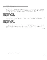
OffBoard PCI IDE Card Uses

This option can only be selected if the 

Onboard IDE

 option is set to 

Disabled.

 You cannot set this option if using the IDE

controller on the motherboard. This option allows you to specify the PCI interrupt that the offboard IDE controller adapter
card uses. The settings are 

INT A, INT B, INT C,

 or 

INT D.

 The Optimal default setting is 

INT A.

Primary Master IDE Block Mode
Primary Slave IDE Block Mode
Secondary Master IDE Block Mode
Secondary Slave IDE Block Mode

When set to 

Enabled,

 these options enable multiple sector reads and writes for the primary master, primary slave, secondary

master, or secondary slave IDE drive. The settings are 

Enabled

 or 

Disabled.

 The Optimal default setting is 

Enabled.

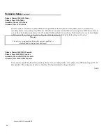
Primary Master IDE PIO Mode
Primary Slave IDE PIO Mode
Secondary Master IDE PIO Mode
Secondary Slave IDE PIO Mode

These options specify the IDE Programmed I/O (PIO) mode used by the primary master, primary slave, secondary master, or
secondary slave IDE drive. The settings are 

Auto

 (AMIBIOS automatically sets the correct IDE mode), 

Mode 0, Mode 1,

Mode 2, Mode 3,

 or 

Mode 4.

 The Optimal default setting is 

Auto.


Selecting a mode not supported by the IDE drive causes

data loss.

Cont'd

Summary of Contents for Super Voyager PCI-II

Page 1: ...American Megatrends Inc Super Voyager PCI II 486 ISA Motherboard User s Guide MAN 724 4 21 95...

Page 2: ...idental or consequential arising from the design or use of this product or the support materials provided with the product Trademarks Intel is a registered trademark of Intel Corporation MS DOS Xenix...

Page 3: ...29 Step 8 Connect the PS 2 Mouse Cable 31 Step 9 Connect Onboard I O 31 Step 10 Install Floppy Drive 32 Step 11 Install Hard Disk 33 Step 12 Install Adapter Cards 34 Step 13 Test and Configure 34 3 AM...

Page 4: ...y with the CPU clock The PCI bus frequency assignments are CPU Internal Clock Frequency PCI Expansion Slots Frequency 100 66 or 33 MHz 33 MHz 75 50 or 25 MHz 25 MHz The PCI bus frequency depends on th...

Page 5: ...pecifications Processor Type and Speed A variety of 486 and 486 overdrive CPUs are supported in both the 168 pin PGA package as well as the 237 pin Intel P24T PGA package including Intel 486DX SX 33 5...

Page 6: ...motherboard supports the Fast ATA specification up to mode 4 L2 Secondary Cache Memory The motherboard supports 128 KB or 256 KB of direct mapped write back L2 external secondary cache memory The exte...

Page 7: ...System BIOS The Super Voyager PCI II 486 ISA motherboard has a 128 KB WINBIOS with built in WINBIOS Setup and user definable hard disk drive types The system BIOS is stored in Flash EPROMs and can be...

Page 8: ...rs for up to four IDE drives with PCI local bus IDE support a 34 pin connector to a floppy controller that supports up to two 720 KB 1 2 MB 1 44 MB or 2 88 MB floppy drives with vertical recording sup...

Page 9: ...IDE Drive Drive Number Drive Letter if One Partition on Drive Drive Letter if Two Partitions on Drive Primary Master 80h C G Primary Slave 81h D H Secondary Master 82h E I Secondary Slave 83h F J IDE...

Page 10: ...upt Levels This motherboard supports the ISA standard 15 hardware interrupt levels The NMI takes precedence over all hardware interrupts IRQs 3 4 5 7 9 10 11 12 14 and 15 can be allocated for use on e...

Page 11: ...able on the ISA bus If enabled onboard peripheral devices use the standard AT I O port address ranges Memory Address on ISA BUS Up to 16 MB of memory can be addressed on the ISA bus Memory Addresses o...

Page 12: ...Super Voyager PCI II 486 ISA Motherboard User s Guide 9 2 Installation...

Page 13: ...instead of the anti static mat A strip of conductive aluminum foil wrapped around the wrist and grounded through a 1 megohm resistor serves the same purpose as the wristband 3 Inside the carton the mo...

Page 14: ...Super Voyager PCI II 486 ISA Motherboard User s Guide 11 Motherboard Layout...

Page 15: ...1 7 Connect the cables Page 32 8 Connect the PS 2 mouse cable Page 34 9 Connect onboard I O Page 34 10 Install floppy drives Page 36 11 Install hard disk drives Page 37 12 Install adapter cards Page 4...

Page 16: ...J2 J3 J6 J8 J9 J10 J11 J12 J13 J14 J15 CPU Selection J7 5V CPU Power J28 J29 3 3V CPU Power J34 Serial Port 1 IRQ Select J35 Serial Port 2 IRQ Select J33 Parallel Port IRQ Select J50 PS 2 Mouse IRQ E...

Page 17: ...A two pin shoring bridge a two pin berg and a shorting bridge also called a jumper mounted on the two pin berg are shown below J42 J44 J45 Cache Memory Configuration J42 J44 and J45 are three pin berg...

Page 18: ...rt Pins 1 2 and 3 4 Short Pins 1 2 and 3 4 Short Pins 1 2 and 3 4 J11 Short Pins 1 2 Short Pins 1 2 Short Pins 1 2 Short Pins 1 2 Short Pins 1 2 J12 OPEN OPEN if WB Short Pins 1 2 if WT OPEN OPEN OPEN...

Page 19: ...2 3 Short Pins 2 3 Short Pins 2 3 J3 OPEN Short Pins 1 2 Short Pins 1 2 OPEN Short Pins 2 3 J6 OPEN Short Pins 1 2 Short Pins 1 2 OPEN Short Pins 1 2 J8 OPEN Short Pins 2 3 OPEN OPEN Short Pins 1 2 J9...

Page 20: ...r AMD using write through caching WT write through mode Setting Jumpers for AMD Plus CPU Caching Modes for L1 Cache Memory The caching mode for the L1 cache memory for AMD CPUs is included in the CPU...

Page 21: ...factory setting Short Pins 1 2 J35 Serial Port 2 IRQ Select J35 is a three pin single inline berg Short pins 2 3 to select IRQ4 for serial port 2 Short pins 1 2 the factory setting to select IRQ3 for...

Page 22: ...s 1 2 DRQ1 Short Pins 2 3 Short Pins 2 3 DRQ3 Short Pins 5 6 Short Pins 5 6 None the factory setting OPEN OPEN J50 Onboard PS 2 Mouse IRQ Select J50 is a three pin single inline berg that selects the...

Page 23: ...that pins 1 2 are shorted before turning power on again If you forget the system password in most computers you must remove the battery for at least 20 minutes to erase CMOS RAM J43 provides a quicker...

Page 24: ...select Flash EPROM present the factory setting short pins 2 3 To select no Flash EPROM present short pins 1 2 Flash EPROM Present J55 Flash EPROM Present factory setting Short Pins 2 3 Flash EPROM Abs...

Page 25: ...s can be used You can mix SIMM types You can use any valid SIMM in any bank The following table provides only some examples of SIMM types It is not an exhaustive list of all valid SIMM combinations Ba...

Page 26: ...he following table provides only some examples of SIMM types It is not an exhaustive list of all valid SIMM combinations Bank1 Bank2 Total DRAM 256 KB x 36 None 1 MB 256 KB x 36 256 KB x 36 2 MB 1 MB...

Page 27: ...firmly push the card into the socket at a 45 degree angle then push it up to a vertical position When properly inserted the SIMM clicks into place as the latching pins engage See the following figure...

Page 28: ...oving the installed CPU and installing a new CPU Make sure all junpers are set correctly You must be absolutely certain of the voltage of the new CPU You must be absolutely certain that the jumpers fo...

Page 29: ...ard figure on page 11 Pin 1 of the socket is on a chamfered corner that corresponds to pin 1 of the CPU also on a chamfered corner Check for bent pins on the CPU Gently straighten any bent pins with a...

Page 30: ...ion screen that appears when the computer starts indicates the CPU type If the new CPU type does not appear reinstall as follows Step Action 1 Turn the power off 2 Check the coprocessor orientation 3...

Page 31: ...The power supply is mounted at the far end of the chassis 3 Push four nylon standoffs from the solder side of the motherboard in the holes provided for them The standoffs lock in place Find the slots...

Page 32: ...y which should have built in filters to suppress radiated emissions Connect to P1 and P2 Attach the cables from the power supply to P1 and P2 on the motherboard as shown below The six pin connector fr...

Page 33: ...Supply Continued Power Supply Connectors are Keyed The power connectors are keyed The connector keys must be cut to fit some power supplies as shown below Important Make sure that the jumpers are con...

Page 34: ...e 31 Step 6 Connect the Keyboard Cable The keyboard connector is a five pin DIN socket labeled KEYBD on the motherboard Attach a standard AT compatible keyboard cable A five pin DIN to six pin miniDIN...

Page 35: ...is indicated on the motherboard by a pointed box around the connector Pin 1 is always at the pointed end of the box as shown below Connect the following cables to the following jumpers on the motherbo...

Page 36: ...ctor J41 is a five pin single inline berg that is attached via a cable to the keyboard lock connector The keyboard lock allows the user to lock the keyboard J54 Turbo LED Connector J54 is a two pin be...

Page 37: ...J21 a parallel port J23 a floppy drive and two IDE connectors The serial and parallel port connectors are described below The floppy connector is described on page 36 The IDE connectors are described...

Page 38: ...I II 486 ISA Motherboard User s Guide 35 Step 9 Connect Onboard I O Continued Attaching the Parallel Port Cable A parallel port cable is supplied to connect J23 to the external parallel port connector...

Page 39: ...to J25 The onboard floppy controller cannot be used if a hard disk adapter card with floppy controller is installed The cable and the connector are shown below The motherboard supports 3 and 5 floppy...

Page 40: ...s Guide 37 Step 11 Install Hard Disk Attach IDE Cable to J22 J22 is the primary IDE Integrated Drive Electronics hard disk drive connector Both the primary master and the primary slave IDE drives mus...

Page 41: ...fer and fast IDE transfer These IDE features are configured in Peripheral Setup in the WINBIOS Setup utility Disable the onboard IDE interface in Peripheral Setup in WINBIOS Setup to use an ISA ESDI R...

Page 42: ...ard is installed Slot1 Slot3 If using only one IDE controller channel and the offboard IDE controller card is in PCI slot1 on the motherboard set Offboard PCI IDE Card Uses to INTA If using both IDE c...

Page 43: ...board WINBIOS If a PCI SCSI Host Adapter card does not have an onboard SCSI BIOS WINBIOS automatically provides the NCR SCSI BIOS on the PCI bus for the SCSI Host Adapter card to use tep 13 Test and C...

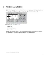
Page 44: ...tup Since WINBIOS Setup resides in the ROM BIOS it is available each time the computer is turned on The main menu screen look like this WINBIOS Setup consists of the following groups Standard Setup Ad...

Page 45: ...he primary master primary slave secondary master and secondary slave If the hard disk drive is an IDE drive select Detect Primary or Detect Slave from the Utility section of the WINBIOS Setup main men...

Page 46: ...p main menu The Advanced Setup options are described below System Keyboard Use this option to specify if error messages are displayed when a keyboard is not attached This option permits you to configu...

Page 47: ...The settings are Enabled or Disabled The Optimal default setting is Disabled System Boot Up Sequence Use this option to specify the boot sequence WINBIOS will boot DOS from either floppy drive A or ha...

Page 48: ...Optimal default setting is Enabled Shadow C800 32K Shadow D000 32K Shadow D800 16K Choose these options to copy the contents of the ROM area named in the option title to RAM The settings for each of...

Page 49: ...are Disabled 64 KB 128 KB 256 KB 512 KB 1 MB 2 MB or 4 MB The Optimal default setting is 2 MB ISA Memory Hole Base Address This option sets the starting address of the ISA memory hole The settings are...

Page 50: ...Time This option allows you to specify the latency for the PCI adapter card in PCI slot 1 The setting can be 1 255 seconds The Optimal default setting is 248 seconds Slot 2 Latency Time This option a...

Page 51: ...Use this option to specify the bus that IRQ7 can be used on The settings are PCI or ISA The Optimal default setting is PCI Assign IRQ 9 To Use this option to specify the bus that IRQ9 can be used on T...

Page 52: ...t setting is PCI Assign IRQ 15 To Use this option to specify the bus that IRQ15 can be used on The settings are PCI or ISA The Optimal default setting is PCI Power Management Setup The WINBIOS Setup o...

Page 53: ...bled The Optimal default setting is Disabled Video Off from Suspend Timeout When this option is set to Enabled VGA adapter cards that have the power down feature can power down when the computer enter...

Page 54: ...ue Power Management option The settings are Monitor or Ignore The Optimal default setting is Monitor Video Activity When this option is set to Monitor the system BIOS monitors all video activity and s...

Page 55: ...his option to Enabled to use the floppy drive controller on the motherboard The settings are Enabled or Disabled The Optimal default setting is Enabled Onboard IDE Set this option to Enabled if using...

Page 56: ...e Secondary Slave IDE Block Mode When set to Enabled these options enable multiple sector reads and writes for the primary master primary slave secondary master or secondary slave IDE drive The settin...

Page 57: ...dard Cylinder Head Sector scheme Data transfer rates can be much higher in LBA mode The settings are Enabled or Disabled The Optimal and Fail Safe default settings are Disabled Warning The drive is re...

Page 58: ...s are running Serial Port 1 Use this option to specify the base I O port address used for onboard serial port 1 The settings are Disabled 2E8h 3F8h or 3E8h The serial port uses eight consecutive I O p...

Page 59: ...56...

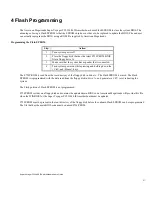
Page 60: ...speaker that is connected 4 Turn system power on while pressing and holding down the Ctrl and Home keys The S724P ROM is read from the root directory of the floppy disk in drive A The Flash EPROM is e...

Page 61: ...Chapter 4 Flash Programming 58...

Page 62: ...che Memory Step Action 1 Turn the system off If the motherboard is already installed in a computer case remove the cover and expose the motherboard 2 Make sure you are properly grounded to prevent ele...

Page 63: ...Appendix A Upgrading Cache Memory 60...

Page 64: ...r Management 43 Board Layout 10 Cache memory configuration 13 Chipset Setup 40 COM1 31 COM2 31 Configuring System 34 Connectors Expansion slots 34 Floppy disk 32 IDE Activity Indicator 30 IDE Hard Dis...

Page 65: ...CPU External Speed Select 20 J31 and J32 Extended Parallel Port DMA Select 18 J33 Parallel Port IRQ Select 17 J34 Serial Port 1 IRQ Select 17 J35 Serial Port 2 IRQ Select 17 J38 Onboard Secondary IDE...

Page 66: ...r Supply 27 Primary Master IDE 32Bit Transfer 48 Primary Master IDE Block Mode 47 Primary Master IDE LBA Mode 48 Primary Master IDE PIO Mode 47 Primary Slave IDE 32Bit Transfer 48 Primary Slave IDE Bl...

Page 67: ...Connector 30 Suspend Timer Value 44 Switch and Jumper Options 12 System Boot Up Num Lock 38 Tables BBS Phone Numbers iv Cache memory support 3 Processor types supported 2 Steps for installing motherbo...

Reviews: