background image

ADM-PCIE-KU3 User Manual


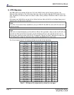
3.3 PCI Express

The ADM-PCIE-KU3 is capable of PCIe Gen 1/2/3 with 1/2/4/8/16 lanes (where 16-lanes requires a two

bifurcated 8-lane interfaces). The FPGA drives these lanes directly using the Integrated PCI Express block from

Xilinx. Negotiation of PCIe link speed and number of lanes used is generally automatic and does not require user

intervention.

PCI Express reset (PERST#) connected to the FPGA at both pins N23 and K22. Do not configure these pins as

outputs and do not add a pull-up constraint.

Note: 

The Xilinx IP core automatically instantiates a pull-up on PERST#, this MUST be removed for the reset pin to

function correctly.

Note: 

Different motherboards/backplanes will benefit from different RX equalization schemes within the PCIe IP core

provided by Xilinx. Alpha Data recommends using the following setting if a user experiences link errors or

training issues with their system: within the IP core generator, change the mode to "Advanced" and open the

"GT Settings" tab, change the "form factor driven insertion loss adjustment" to "chip-to-chip".

The other pin assignments for the high speed lanes are provided in the table below:

Signal

Target FPGA Input

P pin

N pin

PCIE_TX0

MGTHTX3_225

AC4

AC3

PCIE_RX0

MGTHRX3_225

AB2

AB1

PCIE_TX1

MGTHTX2_225

AE4

AE3

PCIE_RX1

MGTHRX2_225

AD2

AD1

PCIE_TX2

MGTHTX1_225

AG4

AG3

PCIE_RX2

MGTHRX1_225

AF2

AF1

PCIE_TX3

MGTHTX0_225

AH6

AH5

PCIE_RX3

MGTHRX0_225

AH2

AH1

PCIE_TX4

MGTHTX3_224

AK6

AK5

PCIE_RX4

MGTHRX3_224

AJ4

AJ3

PCIE_TX5

MGTHTX2_224

AL4

AL3

PCIE_RX5

MGTHRX2_224

AK2

AK1

PCIE_TX6

MGTHTX1_224

AM6

AM5

PCIE_RX6

MGTHRX1_224

AM2

AM1

PCIE_TX7

MGTHTX0_224

AN4

AN3

PCIE_RX7

MGTHRX0_224

AP2

AP1

PCIE_TX8

MGTHTX3_227

G4

G3

PCIE_RX8

MGTHRX3_227

F2

F1

PCIE_TX9

MGTHTX2_227

J4

J3

Table 11 : PCI Express Pin Assignments (continued on next page)

Page 10

Functional Description

ad-ug-1284_v1_13.pdf

Summary of Contents for ADM-PCIE-KU3

Page 1: ...ADM PCIE KU3 User Manual Document Revision 1 13 20th Dec 2018...

Page 2: ...without prior written consent from Alpha Data Parallel Systems Ltd Head Office Address 4 West Silvermills Lane Edinburgh EH3 5BD UK Telephone 44 131 558 2600 Fax 44 131 558 2700 email sales alpha data...

Page 3: ...PCI Express 10 3 4 DDR3 SDRAM SODIMMs 11 3 5 QSFP 12 3 6 SATA 13 3 7 System Monitor 14 3 8 SMA Timing Input 15 3 9 JTAG Front Panel Interface 16 3 10 Configuration 17 3 10 1 Configuration From Flash...

Page 4: ...al Performance 3 Figure 3 ADM PCIE KU3 Block Diagram 4 Figure 4 Switches 5 Figure 5 LEDs 6 Figure 6 Clock Topology 7 Figure 7 QSFP Locations 13 Figure 8 SATA Locations 13 Figure 9 Timing Input Schemat...

Page 5: ...4 8 16 capable x16 requires bifurcation Half length low profile x16 PCIe form factor Two banks of DDR3 SDRAM SODIMM memory with ECC rated at 1600MT s Two right angle SATA connectors SATA3 capable Two...

Page 6: ...e sufficient airflow to cool the FPGA the ADM PCIE KU3 is shipped with a fan on the heatsink The fan is optional and can be easily removed with a Philips screw driver The fan consumes part of the adja...

Page 7: ...he UltraScale tool and set the Device to Kintex UltraScale XCKU060 FFVA1156 2 Extended Set the ambient temperature to your system ambient and select User Override for the Effective Theta JA and enter...

Page 8: ...two SATA3 connectors a SMA input for a timing synchronization input and a robust system monitor XCKU060 2 FFVA1156E 0 4 5 7 8 11 12 15 x16 PCIe Gen3 Edge QSFP Cage 4x10 Gb s HW2 J1 QSFP Cage 4x10 Gb...

Page 9: ...bled SW1 3 OFF Xilinx AD Mode Configure from Alpha Data region Configure from Xilinx region SW1 4 ON Failsafe Default Configure from failsafe region Configure from default region Table 3 SW1 Switch Fu...

Page 10: ...FPGA is not configured D2 CLOCK_LOS Clocks not operating normally Clocks operating normally D3 USR_LED0 User defined 0 pin AE12 User defined 1 pin AE12 D4 USR_LED1 User defined 0 pin AF12 User define...

Page 11: ...ank 47 400MHz Mem Bank 1 IO Bank 45 Fanout PCIe Ref Clock MGTREFCLK0_227 PCIe Ref Clock MGTREFCLK0_225 PC PCIe Ref Clock 100MHz Si5330 Clock Buffer 100MHz 20ppm Source 100MHz Clean PCIe Ref Clock MGTR...

Page 12: ...configuration of the FPGA Signal Target FPGA Input I O Standard pin REFCLK100M IO_L24P_T3U_N10_EMCCLK_65 1V8_CMOS K20 Table 7 EMCCLK 3 2 4 QSFP Clocks The QSFP cages are located in MGT tiles 128 and 2...

Page 13: ...alls that re configure certain frequencies with minimal effort If a user is not using the Alpha Data SDK in their development they can still change these frequencies manually over an I2C interface Sil...

Page 14: ...lowing setting if a user experiences link errors or training issues with their system within the IP core generator change the mode to Advanced and open the GT Settings tab change the form factor drive...

Page 15: ...A3 PCIE_RX15 MGTHRX0_226 Y2 Y1 Table 11 PCI Express Pin Assignments 3 4 DDR3 SDRAM SODIMMs Two DDR3 SDRAM SODIMM connectors can accommodate up to two SODIMMs with 72 bit wide data 64 data 8 ECC Maximu...

Page 16: ...SET_L QSFP0_LP_MODE 31 AF13 AN13 31 QSFP1_LP_MODE QSFP0_MODSEL_L 8 GND GND 8 QSFP1_MODSEL_L QSFP0_INT_L 28 AE13 AN11 28 QSFP1_INT_L QSFP0_MODPRS_L 27 AK13 AP10 27 QSFP1_MODPRS_L Table 12 QSFP Control...

Page 17: ...s connected at this interface Please contact sales alpha data com for more information regarding SATA IP Both RX and TX lines are AC coupled with 10nF capacitors The pin assignments for this interface...

Page 18: ...mperature near maximum 95 degC Warning logged Voltage rail outside recommended values in Kintex Ultrascale Datasheet DS892 Warning logged System Monitor Faults and Responses FPGA Core Temperature abov...

Page 19: ...synchronize multiple cards within a system and to timestamp data Input is on FPGA pin AG11 IOSTANDARD LVCMOS33 The signal is isolated through a optical isolator part number ACPL M61L with a 1 Kohm res...

Page 20: ...without access to the JTAG connector on the PCB a breakout cable can be purchased to bring this connection to the front panel This item is sold separately This item is intended to be used in conjunct...

Page 21: ...flash address map is as detailed below Alpha Data Region Xilinx Reserved Region Region 0 Failsafe 32 MiB Region 2 32 MiB Region 1 Default 32 MiB Region 3 32 MiB Start Address Bytes 0x000_0000 0x200_0...

Page 22: ...erty BITSTREAM CONFIG UNUSEDPIN Pullnone current_design set_property CONFIG_MODE BPI16 current_design set_property CFGBVS GND current_design set_property CONFIG_VOLTAGE 1 8 current_design Generate an...

Page 23: ...te to PCI Express specifying that PERST must not have a pull up removed outdated references to SFP and QSFP Added note in Switches warning users not to use SW1 1 with TI Fusion box 16 Jan 2016 1 7 K R...

Page 24: ...inburgh EH3 5BD UK Telephone 44 131 558 2600 Fax 44 131 558 2700 email sales alpha data com website http www alpha data com Address 611 Corporate Circle Suite H Golden CO 80401 Telephone 303 954 8768...

Reviews: